![]()
Designing pixel readout chips at CERN: From dream to reality.
Back in the 1980s, Erik Heijne at CERN envisioned that the then fledgling integrated circuit technologies could be employed to create a novel radiation detector. His vision was that all the electronics needed for processing signals from a radiation sensor could fit into 1 mm square of silicon. Moreover, he postulated that one could make a two-dimensional array of such circuits on a single electronics chip, with each circuit connecting to its own sensor element, itself part of a 2-dimension array. The sensor and readout electronics chips would form a “sandwich” filled with an array of microscopic solder balls, each one connecting a single detector pixel to its own unique readout pixel. The hybrid pixel detector was born! Michael Campbell explains: “There were two major challenges back then: first, to understand how to design circuits in this new technology and second, to see if it would be possible to make the circuits small enough to turn the hybrid pixel detector from a dream to reality.” Soon, a team of physicists and engineers at CERN in Collaboration with colleagues from the LAA project and the RD-19 Collaboration took up the challenge.
Reading data from the Large Hadron Collider: Developing hybrid pixel detectors.
Twenty years after Erik’s original idea, the LHC started colliding bunches of protons and when the machine reaches its full design regime those bunches will collide 40 million times per second. It is estimated that around 1000 of the 40 million bunch crossings will produce collisions with high enough energy to produce new physics .
To capture all these events and make sure that no information is lost, physicists need very fast cameras which should take around 40 million frames per second! After several levels of triggering, physicists can decide which events are useful for their analysis and where they should look for new particles or other interesting phenomena. Hence, developing new chip technologies was and remains vital for exploring new physics at the LHC.
The birth of the Medipix chips
It was during the evaluation and production of the first prototype hybrid pixel detectors in the early 90’s that the potential of the new technology for applications outside of high energy physics became obvious. As Michael Campbell says: “In particular, in our team we were testing the quality of the bump bonds using radioactive sources and effectively taking pictures of the sources themselves. Sometimes, for fun, we even inserted objects between the source and our detector, forming X-ray images. However, the images were not very nice to look at, because the pixels were rectangular at the time. In addition, the pixel electronics was designed to select only a single frame from many, therefore we had to select and add up a large number of frames to create an x-ray image.”
Michael Campbell and his colleagues decided to make a chip with square pixels and with a kind of camera logic. An electric signal applied to the chip defines how long the shutter will stay open, while a counter in each pixel adds up the total number of particle hits. An image can be created based on these values.
![]()
Illustration of a hybrid pixel detector. It comprises 3 components: a segmented sensor chip connected using solder balls to an identically segmented readout chip.
The Medipix1 chip was produced in 1997, as the outcome of an informal collaboration composed of teams from Freiburg, Germany, Pisa, Italy and Glasgow, Scotland. The chip was fabricated in a 1μm CMOS process, had 4096 square pixels (a matrix of 64 x 64) and covered a sensitive surface of about 11 mm x 11 mm. Medipix1 was used extensively to test a new sensor material, called Gallium Arsenide, which was particularly suited to the detection of X-ray photons in the low energy part of the diagnostic spectrum, a region used in mammography. The chip was also combined with more conventional silicon sensors like those used in physics experiments. As Michael Campbell adds “The main achievement of this chip was to demonstrate the potential of hybrid pixel detectors in fields beyond high energy physics.”
However, the pixel size was a little too big and the number of pixels in the matrix a little too small for many applications. Fortunately, microelectronics technology develops fast and in 1999 a new Collaboration, called Medipix2, was started with the aim of developing a new chip in 0.25μm CMOS. Moving from 1μm CMOS to 0.25μm CMOS chip technology was a major step, but the CERN designers had already accumulated significant experience with the new technology. The readout chip for the ALICE pixel detector (developed at CERN during the late 1990s) was the first LHC pixel chip to use the new process. The other experiments followed that example later. During the development of the Medipix2 chip, the design team was set the task of reducing the pixel size to 50μm, while increasing the number of pixels to 256 x 256. The success of the Medipix1 chip had stimulated a growing interest in this approach, mostly in groups interested in medical imaging applications. Another interesting aspect of the new design was that each pixel was sensitive to charge deposits lying between a lower threshold and an upper threshold; the idea being that it could be used for spectroscopic or “colour” X-ray imaging for the first time. With the Medipix2 chip, hits from one range of x-ray energies can be recorded in one exposure and with multiple exposures one could create a “colour” x-ray image. The first version of the chip was produced in early 2001 and, after various ‘respins’ over the following years, the final version was submitted to production in April 2005. Michael recalls: “During the four years between the submission of the first chip and the final version we learned a lot. Although we had accumulated experience from the ALICE pixel work, our design was many times denser. The tools we used to verify our designs did not give us full coverage for possible errors but, in any case, the Medipix2 chip generated significant scientific output.”
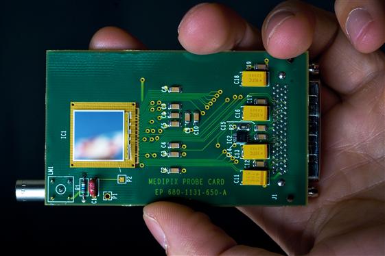
View of the Medipix Card built with an hybrid silicon pixel detectors for tracking applications in High Energy Physics and for imaging applications.
Following the success of Medipix2, physicists from Nikhef, The Netherlands, Bonn, Germany and CEA-Saclay, France (from the EuDet Collaboration) approached the designers to discuss how the chip could be adapted for gaseous detector readout. There was a growing interest to combine Medipix2 technologies with GEM detectors. Reading out the gas detector with the Medipix2 chip provided a kind of binary image of a projection of the particle track from the three dimensional gas volume onto the two dimensions of the pixel matrix. The challenge was to determine where the charges were created in the depth of the gas volume, which meant to make the chip sensitive to the arrival time of the particles in order to produce a 3D image of the track. This request led to the birth of Timepix chip. A clock signal was brought to each pixel and the pixel redesigned such that it could be programmed to work in a number of different modes. In particle arrival mode, the pixel counts the total number of clock ticks, starting from the detection of a particle and stopping when the shutter closes. The timing of the particle arrival reveals where in the gas volume depth it arrived. Alternatively, the counter can be programmed to count the number of clock ticks, while a particle hit is being detected. This mode, is called Time over Threshold (or ToT), and the number of counts in a pixel indicates how much charge has been deposited.
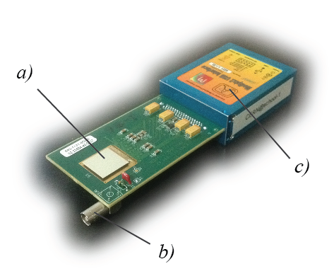
The Timepix hybrid silicon pixel detector. a) is the sensor element, a 300 μm thick silicon wafer with an active area of 1.98 cm2. The upper surface is coated with a thin layer of aluminium foil, while the lower surface is bump bonded to the Timepix readout chip, b) is the High Voltage connection socket; and c) is the Medipix USB Interface which connects the detector to the data acquisition system as well as providing the bias voltage to the sensor element via the High Voltage connection cable. (Image:CERN)
More room for developments…
Timepix images of single X-ray particles of a given energy revealed that the charge measured in a pixel is not perfectly uniform but, on the contrary, it is often spread over several neighbouring pixels.
In order to reconstruct the total deposited energy per hit, especially with the high fluxes common in medical imaging, the group developed new techniques. They decided to use the opportunities offered by a more advanced CMOS process in order to implement a new pixel architecture which used inter-pixel circuitry to mitigate the effects of inter-pixel charge sharing. Prototyping for the new CMOS processes gets more and more expensive, and therefore a new Collaboration, called Medipix3, was formed in 2006.
The Medipix design team was the first to study the use of the 130nm CMOS chip manufacturing technology node for pixel detector readout applications. Following a successful prototyping experience with a small chip, the first full scale prototype was submitted for production in 2008. Michael Campbell notes: “While the small prototype chip had worked perfectly and certain features of the full chip worked well, there were issues with yield (the number of chips without defects) and with an unexplained variation in behaviour from pixel to pixel. It took several years of study and a full new chip iteration to finally have a chip working to its full capacity. This learning phase wasn’t lost time however, as the Medipix team was able to provide hints and advice to other groups, thus saving them much time, money and effort.” These days, the latest version of the Medipix3 chip is being tested and so far it seems to work extremely well.
Every chip needs some means of communicating with a computer. In the days of the Medipix1 chip that task was carried out by using rather heavy, high energy physics readout cards, which were run from an electronics readout crate. Over the years, the Collaborations have moved gradually towards more and more miniaturised readout. The group at the IEAP, Prague has made a particularly strong contribution to the work by developing USB-based readout interfaces, as well as a user friendly interface called Pixelman. Alternative readout systems with high rate and capacity have been developed in various places around Europe, such as the European Light Source ESRF in Grenoble, DESY in Hamburg, the Diamond synchrotron near Oxford and NIKHEF in Amsterdam. Presently, the Medipix3 Collaboration is developing two new chips which point the way to new high energy physics applications. The Timepix3 chip, as its name suggests, builds on the experience gained with the Timepix and Medipix3 chips but it aims to explore a new data push readout scheme. In other words, instead of waiting for instructions to take and read out data, the chip will start spitting out hit information as soon as it starts detecting events. This approach is being evaluated for adaptation to an upgrade of the LHCb vertex detector. The chip will also be used by groups studying new detector concepts for a future linear collider. The Smallpix chip aims to shrink the pixel size, further pushing the limits of the bump bonding interconnect technology towards the dimensions that will be necessary at a future linear collider. Looking ahead, the increased cost of prototyping in even more advanced processes will oblige different groups to pool resources.
Steps to the future…
The hybrid pixel detector technology, which was initially developed for tracking at the Large Hadron Collider, has been adapted to other applications ranging from medical X-ray imaging, radiation monitoring and dosimetry in space, as well as some educational activities and a source for artistic inspiration.
The success of the Collaborations is due to excellent teamwork both within the CERN team and together with the participating institutes. The Medipix Collaborations have grown in an organic way, as new applications have been found for the technology. Collaboration meetings provide an open and friendly forum, where creativity can be stimulated by the mingling of minds and cultures from different areas of research. Michael Campbell says: “The growth of the Collaborations has permitted us to pool resources and to continue to exploit the latest CMOS processes available. It has also allowed us to do more than we had originally foreseen, permitting new chips and techniques, which would be financially infeasible for individual groups otherwise, to be developed”. In addition, an important, but often underestimated feature has been a legal framework for the Collaborations, which seeks to permit the creative mingling of ideas while protecting and acknowledging those whose intellectual property is ultimately commercialised. The professional and rigorous legal and commercial support by members of CERN’s various Technology and Knowledge Transfer Departments have played a major role.
Serendipity has also been very important for the success of the project. After all, many applications were entirely unforeseen in the beginning of our work. Collaboration between different fields of science can be, and in our case has proven to be, a winning formula.
For more information about Medipix you can visit the Collaboration's website where you can find more information about past and current projects as well as read more about the future plans of the collaboration: http://medipix.web.cern.ch/medipix/