![]()
RD53: Making the challenging pixel detector chips for the Phase-II upgrades of ATLAS and CMS
The RD53 collaboration has developed over the last five years the foundations to make the extremely challenging pixel detector chips for the Phase-II pixel upgrades of ATLAS and CMS. A large-scale demonstrator chip, called RD53A, was produced last year and during the last six months has been undergoing successful extended tests. The design of the final production versions of the pixel chips for the two experiments is currently ongoing and the scheduled submission is for next year.
Higher resolution tracking with pixel detectors will be vital to reconstruct events at the high collision rates at the HL-LHC with the very high track densities expected (thousands per 25ns bunch crossing). The successful use of hybrid pixel detectors in the current LHC experiments has been a major achievement enabling a rich and successful physics program. Next generation pixel detectors pose new major challenges that require significant advances in many aspects of pixel detectors, starting with their highly integrated readout electronics.
The HL-LHC pixel upgrades requires ~5 times higher granularity (pixel size of 50x50um2), at an order of magnitude higher hit rates of up to of 3GHz/cm2, with analog charge readout to get very good tracking resolution. To perform efficient event selection, under the very challenging conditions of the HL-LHC, trigger rates will be increased by an order of magnitude and the trigger latency increased by a factor ~5. This combination of requirements pose severe challenges for the pixel readout integrated circuit being located in the most hostile environment ever at the heart of the experiments with radiation levels reaching 1Grad over ten years for the inner most pixel layers. This must in addition be obtained at reduced material budget, requiring the use of a novel serial powering concept, with complete power regulation and power conditioning on the pixel chip itself, in combination with highly efficient CO2 cooling systems.
The RD53 collaboration has during its first three years developed and prototyped a multitude of required basic building blocks (analog front-ends, DACs, ADC, shunt-LDO power regulator, etc.) in the chosen 65nm CMOS technology, which was new to our community. Different chip architectures have been evaluated and extensively simulated with a dedicated RD53 pixel chip simulation and verification framework. Finally, a large effort has been invested to get a better understanding of radiation effects in the extremely hostile radiation environment in the pixel detectors. Analog and digital test chips have been designed and characterized for radiation effects at different biasing and temperature conditions. Radiation damage above 100Mrad levels can be severe, especially for small transistors required in high-density digital logic and data buffering. It was realized that effective radiation damage can become both reduced or amplified by annealing depending strongly on annealing conditions (biasing and temperature). The fact that the pixel detectors will be operating cold (-20oC), and only biased/powered when cooled, will play a major role in limiting effective radiation damage. This allows pixel chips to be made with appropriate design techniques to tolerate at least 500Mrad, implying that inner pixel layers may have to be exchanged after five years of operation. Further extensive radiation tests of the RD53A demonstrator will show if it is viable to have complex mixed signal pixel chips operating up to 1Grad.
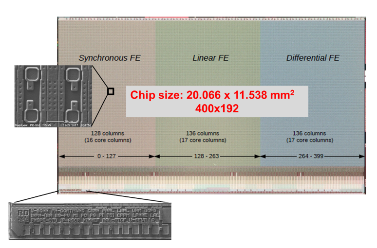
A picture of the RD53A chip.
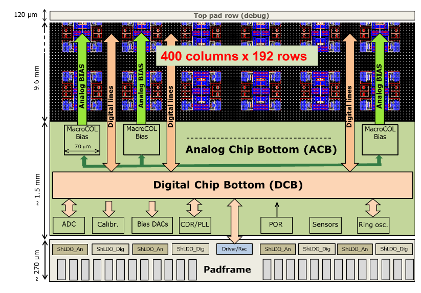
The block diagram of the RD53A chip
The last two years have been focused on designing and submitting the RD53A demonstrator pixel chip. This demonstrator chip is designed as being a full sized pixel chip with all main/critical functions included. In the end the chip was submitted as a half-sized chip (2cm x 1cm) to allow mask sharing with another large tracker chip, the CMS MPA chip, as mask costs of a modern 65nm CMOS technology is significant. The RD53A chip contains specific test functions to allow direct comparisons of three alternative implementations of low power analog front-ends and dedicated functions to measure radiation effects. The RD53A chip has since the beginning of this year been extensively tested by the RD53 community and has been found fully functional. Chips and RD53 developed test systems are now being distributed across the ATLAS and CMS pixel communities for extensive testing, characterization and verification of pixel sensors, serial powering and realistic pixel modules for large-scale pixel detector system tests.
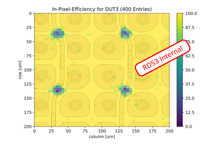
First preliminary test of a pixel sensor detection efficiency, with the RD53A chip in a CERN test beam in May 2018. The observed holes on hit efficiency is due to a specific biasing applied to tests the behaviour of the pixel sensor. as expected the hit efficiency under this specific biasing condition is low at these areas, validating the behaviour of the RD53A chip down to the sub-pixel level.
Concurrently to testing the RD53A chip, the RD53 chip design team has prepared an improved design framework to make the final production chips for both ATLAS and CMS. Since the foundation of the RD53 collaboration in 2013, some of the requirements from the two experiments have evolved differently (e.g. trigger rates and latencies). It has been determined that an appropriate common architecture can accommodate such differences. Differences in the pixel detector layouts of the two experiments (e.g. CMS pixel detector being closer to beam, ATLAS pixel detector being bigger, etc.) dictates that dedicated pixel chips of different size and aspect ratio are required. The improved RD53 design framework can map the common pixel chip architecture into two chip implementations of different size, controlled by a few key parameters in design generation and verification scripts. Both chips could in principle be submitted at the same time but it has been decided to time skew the two submissions to reduce cost risks related to potential design problems. The ATLAS sized chip will be submitted ~mid 2019 and after basic verification of this chip (also by CMS groups) the CMS sized chip will be submitted ~end 2019.
The RD53 collaboration consists of 22 institutes across the European and American continents. Designing, verifying and testing so challenging complex mixed signal chips across so many different groups, people and experiment boundaries has been a challenging but also a very rewarding experience for everybody taking part in this. There has been a lot of exchange of experience and ideas during the years, which has benefitted significantly the two pixel projects and everybody contributing to this. An excellent collaboration spirit, weekly and well-organized meetings combined with getting the core design team together at CERN for several months before the RD53A submission has been the recipe to make this successful.
RD53 institutes: Aragon, Bari, Bergamo-Pavia, Bergen, Bonn, CERN, CPPM, Fermilab, LAL-Orsay, LBNL, LPNHE Paris, Milano, NIKHEF, New Mexico, Padua, Perugia, Pisa, Prague, RAL, Santa-Cruz, Seville, Torino.
Further reading:
Latest RD53 LHCC report: here.
ACES presentation of RD53: here.
ACES presentation of CMS and ATLAS pixels upgrades: here.
ACES presentation of serial powering: here.
RD53 Indico for workshop and conference presentations: here.