![]()
Silicon photonics for high-energy physics experiments
Optical links have become ubiquitous in High Energy Physics (HEP) experiments to transport data generated from the particle detectors and other control points along the accelerator to the processing electronics. So far, links based on both single-mode Edge Emitting Lasers (EELs) [1] and multi-mode Vertical Cavity Surface Emitting Lasers (VCSELs) [2] are in us. The drawback of these laser diode-based technologies is their degradation due to displacement damage from particle fluence [3]. With the ever-higher radiation levels and the increasing data volumes, alternatives have to be investigated. In the innermost detector regions the challenge is not only to withstand the high radiation levels but also to satisfy the space restraints which make highly integrated links necessary. Silicon Photonics seems to be a quite promising candidate addressing all those points and is currently being investigated for its applicability for use in optical links in future HEP experiments.
Silicon photonics is a highly integrated platform where all photonic components like photodetectors, modulators, lasers and the electronics are grown or implemented on the same piece of silicon. Silicon On Insulator (SOI) wafers in combination with well-established CMOS processes are used for the production. The compatibility with CMOS electronics opens the door to highly integrate the optical links within the detector system. In order to achieve this goal it has to be made sure that optical links based on silicon photonics can perform in and withstand the harsh conditions of the HEP experiments and at the same time can satisfy the challenges of low power consumption and high data rates.
In a first step, the radiation resistance of the building blocks of a silicon photonics optical link, which are modulators, photodiodes and waveguides have been investigated. While we found that all tested devices are very resistant against displacement damage, modulators unfortunately show a strong degradation due to ionizing radiation [4]. A silicon photonics test chip was designed by us (Figure 1), including different passive structures as well as modulator and photodiode structures [5]. Numerous irradiation tests and simulations have been performed to better understand the effects and to overcome the degradation due to total ionizing dose. We showed that it is possible to increase the radiation resistance by design [6] and that an additional increase can be achieved when the devices are operated at low temperatures [7].
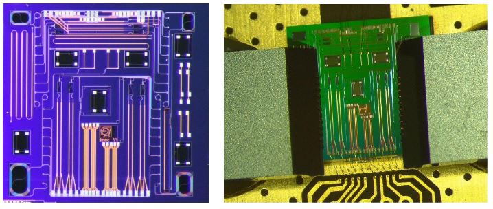
Figure 1: Silicon Photonics test chip designed by the Opto team of the EP-ESE-BE section. Bare chip (left) and including electrical and optical assembly (right).
Throughout the investigations, we found a very efficient annealing effect of the irradiated modulators, applying a forward bias [7]. This leads to a full recovery after irradiation, which was proven by re-irradiation tests. But also, we showed that a high enough current for a sufficient time period prevents the radiation induced degradation already during irradiation [8]. As the standard operation of these modulators (depletion type modulator) is in reverse bias it is not possible to anneal the devices during their operation but in phases where the operation of the HEP experiments is paused eg. during shut-downs, technical stops or interfills the annealing could be performed.
In this first technology evaluation period the focus was mainly on so called Mach-Zehnder Modulators. While these devices come with many advantages such as stability towards manufacturing errors, temperature and wavelength drift as well as already very well proven systems based on MZMs they also come with some drawbacks. First of all a rather large size (more than 1 mm) is necessary to reach the desired efficiency and this comes hand in hand with quite high biasing voltages and high optical losses. All of this leads to a high power consumption. One alternative could be the so-called Ring Modulator [9], which gains more and more attention in the silicon photonics community. Due to the smaller size (negligible optical loss) and higher tuning efficiency, the power consumption can be reduced. The only disadvantage is the high sensitivity to temperature and manufacturing variations, which makes a control loop including a local heater necessary. However, this also brings some positive effect. The possibility of tuning the resonant frequency combined with their small size, ring modulators are very attractive for use in multi-channel systems like wavelength division multiplexing (WDM) [10].

Figure 2: Microscope image of a Ring Modulator.
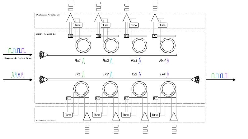
Figure 3: Schematic of a ring modulator WDM transceiver. Ring resonators with different and tuneable resonator wavelengths are located along horizontally drawn bus waveguides.
Further Reading:
[1] J. Troska et al., “Optical readout and control systems for the CMS tracker,” IEEE Trans. Nucl. Sci., vol. 50, no. 4 II, pp. 1067–1072, 2003.
[2] J. Troska, S. Detraz, S. S. El Nasr-storey, P. Stejskal, C. Sigaud, and C. Soos, “Radiation Damage Studies of Lasers and Photodiodes for Use in Multi-Gb / s Optical Data Links,” IEEE Trans. Nucl. Sci., vol. 58, no. 6, pp. 3103–3110, 2011.
[3] S. S. El Nasr-Storey et al., “Irradiation of new optoelectronic components for HL-LHC data transmission links,” J. Instrum., vol. 8, no. 12, pp. C12040–C12040, Dec. 2013.
[4] S. S. El Nasr-Storey et al., “Neutron and X-ray irradiation of silicon based Mach-Zehnder modulators,” J. Instrum., vol. 10, no. 03, pp. C03040–C03040, Mar. 2015.
[5] M. Zeiler et al., “Design of Si-Photonic structures to evaluate their radiation hardness dependence on design parameters,” J. Instrum., vol. 11, 2016.
[6] M. Zeiler et al., “Radiation Damage in Silicon Photonic Mach–Zehnder Modulators and Photodiodes,” IEEE Trans. Nucl. Sci., vol. 64, no. 11, pp. 2794–2801, Nov. 2017.
[7] A. Kraxner et al., “Investigation of the Influence of Temperature and Annealing on the Radiation Hardness of Silicon Mach–Zehnder Modulators,” IEEE Trans. Nucl. Sci., vol. 65, no. 8, pp. 1624–1631, Aug. 2018.
[8] A. Kraxner et al., “Radiation tolerance enhancement of silicon photonics for HEP applications,” in Topical Workshop on Electronics for Particle Physics (TWEPP2018), 2018, vol. 343, p. 150.
[9] G. Li et al., “Ring Resonator Modulators in Silicon for Interchip Photonic Links,” IEEE J. Sel. Top. Quantum Electron., vol. 19, no. 6, pp. 95–113, Nov. 2013.
[10] H. Li et al., “A 25 Gb/s, 4.4 V-Swing, AC-Coupled Ring Modulator-Based WDM Transmitter with Wavelength Stabilization in 65 nm CMOS,” IEEE J. Solid-State Circuits, vol. 50, no. 12, pp. 3145–3159, Dec. 2015.