
A Hundred Gigabits per Fibre: Silicon Photonics Links for the Detectors of Tomorrow
by WP6 HIGH SPEED LINKS TEAM, EP-ESE, CERN

Every time two proton beams collide at the centre of a Large Hadron Collider experiment, a burst of particles radiates outward at nearly the speed of light, leaving trails through layers of precision detectors. Each detector element (whether a silicon pixel, a calorimeter crystal, or a muon drift tube) must record what it sees and pass that information to counting rooms hundreds of metres away, where computers can reconstruct what happened in the collision. This is already a demanding engineering challenge, and the EP R&D programme was conceived in the context of future experiments pushing these demands far beyond what existing technology can deliver.
With construction of the High-Luminosity LHC (HL-LHC) now well underway, the scale of that challenge is becoming concrete. The HL-LHC will increase the collision rate by a factor of five to ten compared to the LHC design. Future detectors, such as those planned for LHCb and ALICE upgrades, will push requirements still further. The result is a rapid growth in the volume of raw data that must travel from inside the detector, centimetres from the interaction point and exposed to intense radiation, to counting rooms hundreds of metres away. The on-detector electronics must transmit data faster, while surviving radiation doses that would destroy commercial chips, all while consuming less power and adding as little material as possible to the detector. This is the central problem that the High Speed Links (HSL) Work Package, WP6 of the EP R&D programme, is working to solve.
Why optical links, and why Silicon Photonics?
Optical fibres are the natural medium for transmitting data over tens or hundreds of metres at high bandwidth: they are lightweight, immune to electromagnetic interference, and capable of carrying data at speeds far exceeding what copper cables can reliably achieve at long range. The LHC and HL-LHC experiments already rely on optical links for detector readout, using Vertical Cavity Surface-Emitting Lasers (VCSELs) to convert electrical signals to light. One of the VCSELs’ fundamental limitations is their modest radiation tolerance, allowing them to survive only up to about 1 MGy of total ionising dose. Next-generation detectors will expose on-detector electronics to doses exceeding what VCSELs can withstand, and therefore a new optical transmitter technology is needed.
Silicon Photonics (SiPh) technology offers a compelling alternative. Instead of using a laser directly on the detector, the idea is to keep the optical power source safely off the detector where it is not exposed to radiation. Unmodulated light is guided into the detector via optical fibre and a small on-detector device imprints the data signal onto that light by modulating its intensity. This modulator (implemented as a micro-ring resonator etched into a silicon photonic chip) is expected to be more than an order of magnitude more radiation tolerant than a VCSEL and can be fabricated using industrial silicon processes already available through commercial foundries. By combining Wavelength-Division Multiplexing (WDM), in which multiple laser wavelengths travel simultaneously through a single fibre, the aggregate data bandwidth per fibre can reach 100 Gbps.
This is the architecture WP6 is developing: commercial off-the-shelf laser sources, each emitting at a different wavelength, are combined off-detector into a single fibre and fed to an on-detector Photonic Integrated Circuit (PIC), which selectively modulates each wavelength with a different data channel. The modulated light travels back through the fibre to commercial receivers and Field Programmable Gate Arrays (FPGAs) in the back-end, where the data are reconstructed. Custom radiation-hardened ASICs drive the PIC and serialise the data from the detector front-end. The result is a fully optical, high-bandwidth, radiation-tolerant readout link that leverages the commercial ecosystem of the data centre industry wherever possible, and adds custom radiation-hardened technology only where strictly necessary.
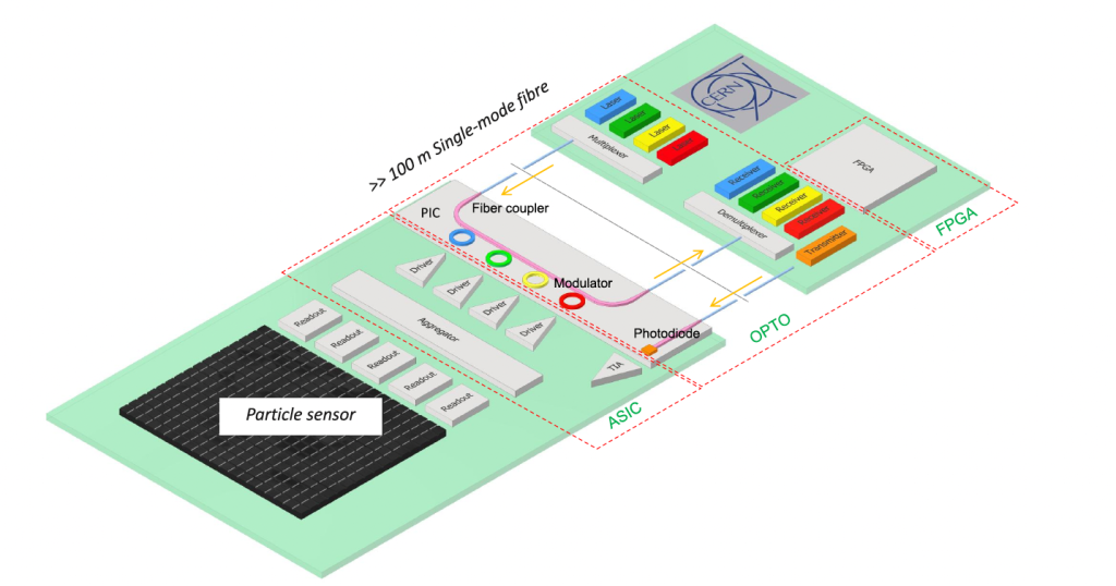
Figure 1: The WP6 link architecture. Commercial multi-wavelength laser sources are combined off-detector into a single fibre. An on-detector SiPh PIC modulates each wavelength with one data channel. The modulated light is received by a commercial FPGA-based back-end. Custom radiation-hardened ASICs drive the PIC and serialise the detector data.
This work is already taking shape in a real experiment context. The PicoPix pixel detector, destined for the VELO-II vertex detector at the LHCb, is one of the first target platforms for WP6’s optical link technology. Building the full system requires solving problems across three distinct but deeply interconnected domains: the design of radiation-tolerant custom ASICs, the evaluation of commercial FPGA-based back-end systems, and the development of Silicon Photonics components and their packaging. WP6 has organised its work accordingly, running three parallel activities that are now converging toward integrated system demonstrations.
ASIC developments: driving the photonics at 100 Gbps
The ASIC activity is responsible for the custom integrated circuits that interface the detector front-end electronics to the on-detector optical modulator. The central achievement of the first phase of R&D was the DART28 ASIC: a four-channel data transmitter fabricated in 28 nm bulk CMOS, capable of sending data at 25.6 Gbps per channel and surviving total ionising doses exceeding 10 MGy, with exceptional tolerance to single-event effects. DART28 demonstrated, for the first time in the HEP community, that commercial 28 nm CMOS technology can be used to build the high-speed optical transmitters that future detector readout demands. Its all-digital phase-locked loop, a novel architecture that replaces conventional analogue control circuits with a fully digital implementation, achieved a random jitter below 300 fs, almost ten times better than the previous generation of HEP links, while remaining fully functional after 20 MGy of X-ray irradiation [1, 2].
Characterising the DART28 ASIC in conjunction with the photonic devices developed by the SiPh team was an essential step in understanding the full system requirements. This joint work revealed that reliable ring modulator operation requires a driver output swing of at least 2.5 V, significantly larger than the output of the DART28 driver operating from the standard 0.9 V supply of 28 nm CMOS. This gap drove the design of the SPRINT macro-cell (Silicon Photonics Radiation-Tolerant Integrated Transmitter), now in the final stage of development. SPRINT’s centrepiece is a novel high-voltage driver that achieves a 3.6 V output swing using only standard thin-oxide 28 nm transistors, the kind individually rated for just 0.9 V. This is accomplished through a multi-voltage-domain architecture, in which four stacked voltage domains internally share and transfer electrical charge to generate the high swing at the output while never exceeding the voltage rating of any individual transistor. The result is a circuit innovation: the driver delivers nearly four times the output swing of its predecessor while simultaneously reducing current consumption by a factor of four, and it is designed for operation at up to 10 MGy total ionising dose. Post-layout simulations confirm open-eye diagrams at 25.6 Gbps across all process corners and across the full industrial temperature range (−40 to 125 °C), with an average power consumption of approximately 83 mW [3].
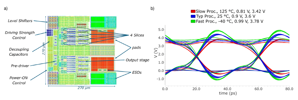
Figure 2: The high-voltage driver developed for SPRINT. Left: chip layout including decoupling capacitors, bond pads, and ESD protection circuits. Right: simulated output eye diagrams at 25.6 Gbps for three process corners, with the driver connected to the SiPh micro-ring modulator via a 500 𝜇m bond wire. The 0–3.6 V swing is achieved using only thin-oxide 28 nm devices.
Because micro-ring modulators are thermally sensitive (their resonant wavelength shifts with temperature and can drift out of alignment with the laser), each channel in SPRINT is accompanied by a Temperature Control Unit (TCU). The TCU continuously monitors the optical power absorbed by the ring modulator through an integrated photodiode and adjusts the current through a micro-heater to lock the modulator’s resonant frequency to the designated laser wavelength, ensuring maximum optical modulation efficiency. This closed-loop thermal stabilisation is essential for reliable data transmission, as ambient temperature fluctuations in a real detector environment continuously shift the modulator’s resonant wavelength. Total ionising dose is expected to produce a similar effect, introducing an additional wavelength drift that the TCU will also compensate. The TCU architecture features a current-input delta-sigma analogue-to-digital converter achieving approximately 9 bits of effective resolution and a high-power output stage capable of delivering more than 80 mW to the heater with sub-100 μW power resolution. To validate the concept before committing it to silicon, a prototyping platform combining an FPGA, discrete analogue components, and a real photonic integrated circuit was built in the laboratory and used to demonstrate initial locking of the control loop under realistic operating conditions [4].
A dedicated study of power delivery network integrity (a contributing factor to the jitter observed in DART28 prototype testing) has produced recommendations for the signal and power interconnects between the SPRINT macro-cell and its carrier board, helping to ensure that the resonance-induced errors seen in DART28 do not recur [5]. In parallel, behavioural-level integration of SPRINT into the PicoPix architecture has been completed, data format compatibility has been verified through simulation, and the design is progressing toward a joint ASIC submission.
FPGA developments: precision timing and next-generation back-end readout
Commercial FPGAs serve as the back-end counterpart to the custom front-end ASICs. They receive, process, and route the data arriving from the detector over the optical links, and distribute control and clock signals back to the front-end. In the HL-LHC and beyond, FPGAs must handle aggregate bandwidths of Terabits per second while maintaining timing precision at the level of a picosecond or better. WP6’s FPGA activity addresses both of these requirements.
The timing challenge is perhaps the more subtle one. HEP experiments depend on precise synchronisation across a distributed detector system spanning many tens of metres. Clock signals must be distributed from a central source to every front-end electronics board and the phase of the transmitted data must remain stable to a few picoseconds relative to the reference clock even as board temperatures fluctuate during operation. Current commercial FPGAs introduce phase instabilities that future experiments may no longer be able to tolerate.
WP6’s PSLink project addresses this with a hardware approach that bypasses the FPGA’s intrinsic sensitivities entirely. Phase monitoring is implemented on the data links themselves using discrete components mounted around the FPGA, rather than inside the fabric where temperature-sensitive resources generate instability. The key measurement technique is a Digital Dual Mixer Time Difference (DDMTD) which compares two clock signals using a time-amplification technique that achieves sub-picosecond resolution. Two variants of a dedicated PSLink PCB mezzanine were designed and characterised. The first implements the original technique in which clocks recovered from the data streams are compared by the DDMTD. The second version applies the phase measurement directly to the raw data stream using a novel DDMTD architecture. The new datastream DDMTD was characterised on a Virtex UltraScale+ FPGA and demonstrated a phase measurement residual error of 0.35 ps RMS on live multi-Gbps data [6].
Separately, the transmitter phase aligner firmware module (which achieves deterministic transmitter phase at each restart by controlling the phase interpolator of the FPGA transceiver) was ported to the latest AMD Versal FPGA family. Demonstrations on both Versal Prime and Versal Premium devices achieved phase reproducibility of 0.3 ps RMS across full transceiver resets, matching the best performance previously demonstrated on other FPGA families and confirming that picosecond-level timing determinism is achievable on the newest commercial devices.
The bandwidth challenge is being addressed through the study of the applicability of 100 Gigabit Ethernet for Front-End (100GbE4FE) systems. The premise is straightforward but ambitious: rather than designing yet another custom HEP readout protocol (as was done for lpGBT, or as is the case for the bespoke interface in SPRINT), can detector data be transmitted from the front-end directly using the same 100 Gbps Ethernet standard that governs data centre networking? If so, the entire commercial ecosystem of switches, network interface cards, cables, and software becomes available for HEP readout at commodity prices. As with any approach borrowed from a different domain, there are open technical questions to address, among them the behaviour of commercial error-correction schemes under radiation, the compatibility with existing detector timing infrastructure, and the path to full system integration. These are being studied systematically within WP6 [7].
A major effort concerned practical protocol conversion: translating data from existing lpGBT-based front-end links into 100 Gbps Ethernet packets, enabling detectors instrumented with current-generation links to connect directly to a commodity Ethernet network. Two hardware form factors have been developed: a single-link SFP module operating at 10 Gbps, and a quad-link QSFP module offering 40 Gbps of aggregate bandwidth in a housing that plugs directly into a standard commercial Ethernet switch, providing a cost-efficient bridge between the HEP detector world and the data centre world. New firmware handles the task of sorting and reassembling data fragments from multiple lpGBT links into contiguous data blocks suited to CPU and GPU processing. An auto-configuration system ensures that each converter module can identify itself to a central database server at startup and automatically load its configuration, making the system practical to deploy at scale without per-module firmware customisation. First QSFP prototypes have been successfully operated, with firmware being tested and validated.
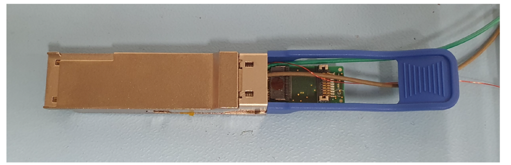
Figure 3: Prototype QSFP module developed within WP6 for quad-lpGBT to 40 Gbps protocol conversion. The module plugs directly into a standard commercial Ethernet switch, providing a cost-efficient bridge between the detector front-end and a commodity data centre network.
Silicon Photonics: demonstrating the optical link and surviving radiation
The SiPh activity develops the photonic integrated circuits at the heart of the optical link concept and characterises their radiation tolerance. Recent work marked a turning point: the two PICs fabricated in the previous phase (PackagingPIC and SystemPIC) were fully characterised, a series of irradiation campaigns deepened understanding of radiation effects, and a new photonic chip was designed and submitted for fabrication.
The most significant system result was the first demonstration of a complete four-channel CWDM4 optical transmitter operating at 25.6 Gbps per channel using the micro-ring modulators integrated in the SystemPIC. Four unmodulated laser wavelengths, spanning the CWDM4 band from 1271 nm to 1331 nm, were coupled into the PIC from a commercial External Laser Source module in the standard QSFP form factor, identical to those used in data centre transceivers. All four ring modulators were simultaneously modulated with a pseudo-random bit sequence at 25.6 Gbps and wide-open optical eye diagrams were obtained at all four channels with good amplitude uniformity across the full wavelength band. This demonstration validates the core of the WP6 link concept: a single PIC carrying four wavelength-multiplexed channels at 25.6 Gbps each, for a total of 100 Gbps over a single fibre, with all optical power supplied by a commercial source positioned safely off the detector. Compatibility with a standard commercial QSFP receiver at the back-end was also demonstrated [8].
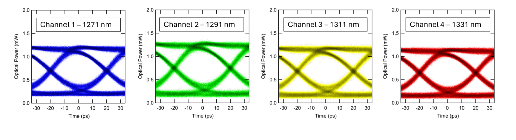
Figure 4: Optical eye diagrams at 25.6 Gbps measured simultaneously at all four micro-ring modulator outputs of the SystemPIC, spanning the CWDM4 wavelength band (1271–1331 nm). The wide-open eyes at all four channels confirm reliable data transmission and good uniformity across wavelengths.
Three irradiation campaigns addressed the radiation tolerance of the photonic components. In the first, micro-ring modulators were exposed to X-ray doses reaching 12.3 MGy while their electro-optic frequency response was measured in situ. While radiation degrades the high-frequency response of the ring modulator, a key finding is that this damage is almost completely reversible: localised thermal annealing using the integrated micro-heater for approximately one hour anneals the radiation-induced defects and restores near-original performance without raising the temperature of the whole PIC [9]. This means that periodic localised annealing during scheduled experiment technical stops can maintain link performance throughout the detector’s lifetime, without risking data-taking.
The second campaign, using neutrons at the Cyclotron Resource Centre of UCLouvain in Belgium, measured radiation-induced attenuation in silicon waveguides at fluences up to 7 × 10¹⁵ n/cm². While attenuation is non-negligible in the most sensitive waveguide types (reaching approximately 0.6 dB/mm per 7 × 10¹⁵ n/cm²), it is manageable in a well-designed optical power budget, particularly since photobleaching partially mitigates the effect during operation [10]. A third campaign discovered significant and potentially beneficial reductions in nonlinear optical loss in waveguides under combined ionising and displacement-damage irradiation, a finding relevant both to HEP applications and more broadly to the Silicon Photonics community.
The next-generation photonic chip, PIC4links, integrates four-channel transmitters using CERN-developed micro-ring modulator blocks, together with novel on-chip passband optical filters that enable automatic wavelength locking, the mechanism by which each modulator automatically identifies and stabilises to its designated laser wavelength. Two filter variants are included: one in the conventional silicon optical layer (previously prototyped and measured in the PackagingPIC), and a novel design in a silicon nitride layer newly offered by the foundry, which provides improved manufacturing tolerances and enables edge couplers compatible with standard single-mode and polarisation-maintaining fibres. This compatibility with off-the-shelf fibre assemblies substantially reduces packaging cost and complexity. The pad frame of PIC4links was co-designed with the SPRINT macro-cell to ensure wire-bond assembly compatibility, making PIC4links the intended photonic counterpart for the PicoPix-based system demonstrator.
Packaging: bridging the electrical and optical worlds
A photonic chip that performs well on an optical probe station must ultimately be reliably assembled into a detector module. Photonic packaging (attaching optical fibres to a PIC with sub-micron alignment precision, wire-bonding the PIC to the readout ASIC, and ensuring the assembly survives vibration and thermal cycling) is one of the most challenging aspects of the entire development, and has historically been a limiting factor for Silicon Photonics in scientific applications.
WP6 invested in a custom six-axis fibre alignment and attachment machine, procured in 2024 and now operating routinely in the laboratory. The machine actively aligns a fibre array to the PIC using optical feedback and cures a UV-epoxy bond to lock the alignment permanently. It has demonstrated sub-decibel repeatability in optical insertion loss across hundreds of alignment runs, a key benchmark for establishing a reliable and repeatable packaging process. The machine is used both to assemble test structures for irradiation studies and as a precision optical probe station for PIC characterisation.
A notable milestone was the assembly of a demonstrator in which the Timepix4 readout chip was co-packaged with the SystemPIC: the ASIC’s serial output (operating at 10 Gbps via a driver not optimised for driving ring modulators) was connected to the micro-ring modulator via a wire bond approximately 600 μm long, and a commercial fibre array was actively aligned and attached to the PIC. This assembly is the first realisation of the low-mass optical readout concept being developed within WP6, in which a photonic chiplet is directly bonded beside the sensor readout chip, eliminating intermediate electrical interfaces and minimising the material added to the detector.
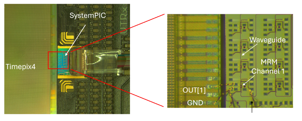
Figure 5: Demonstrator of the Timepix4 readout chip co-packaged with the SystemPIC. A micro-ring modulator is wire-bonded to a Timepix4 serial output with a bond length of approximately 600 𝜇m. A commercial eight-fibre array (two fibres used) is actively aligned and attached to the PIC. This assembly demonstrates the low-mass co-packaging concept at the heart of the WP6 development.
The PicoPix and PIC4links assembly planned for the next phase will take this concept to its next level of integration, with the SPRINT macro-cell directly wire-bonded to PIC4links and fibres edge-coupled to the PIC, delivering a complete 100 Gbps optical transmitter module cointegrated with the pixel detector. Packaging activities are supported by a supply chain effort to identify optical fibre assemblies, adhesives, and connectors compatible with the long-term operation requirements of particle detector environments, including low-outgassing and extended temperature range specifications
Looking ahead: from building blocks to system demonstrators
WP6 began as a component-level R&D programme, and it has been highly successful in that phase. The individual building blocks are now in place: a radiation-tolerant 25.6 Gbps ASIC transmitter, a four-channel Silicon Photonics PIC operating across the CWDM4 wavelength band, a high-voltage driver capable of 3.6 V swing at 25.6 Gbps, a closed-loop thermal control system for wavelength stabilisation, reliable photonic packaging processes, and back-end firmware tools for picosecond-level timing and data handling.
The programme is now entering a new phase, in which these building blocks must be integrated into complete, end-to-end system demonstrators. The integration of SPRINT into PicoPix, the assembly of PIC4links with the SPRINT driver using the co-designed bond pad frame, and the closure of the thermal control feedback loop between the photonic chip and the ASIC are all targeted for the near future. The result will be a radiation-hard optical link integrated with a pixel detector readout chip via a single optical fibre, carrying 100 Gbps across four CWDM4 wavelengths. In parallel, the downlink direction (carrying clock and control signals from the counting room to the detector) is being addressed through the development of a Transimpedance Amplifier (TIA) and a Clock and Data Recovery (CDR) circuit, completing the set of building blocks required for a fully bidirectional optical link.
The broader implications extend well beyond any single detector project. Silicon Photonics-based optical links, with their combination of high bandwidth, radiation tolerance, and compatibility with the commercial data centre ecosystem, are emerging as the most credible technology path for the optical readout of next-generation HEP detectors. By developing the know-how, the components, and the integration processes now, while there is still time to validate and iterate before the experiments demand it, WP6 is ensuring that this technology will be ready when needed.
References
[1] A. Klekotko, S. Biereigel, M. Baszczyk, P. Moreira, F. Martina, J. Prinzie, and S. Kulis. “A radiation-tolerant 25.6-Gb/s high-speed transmitter in 28-nm CMOS with a tolerance of 1 Grad.” IEEE Transactions on Nuclear Science, 71(9):2124–2132, 2024.
[2] S. Biereigel, S. Kulis, and P. Moreira. “All-digital phase-locked loop with single-event phase and frequency transient suppression.” In Proceedings of RADECS 2025, Antwerp, Belgium, 2025.
[3] Gabriele Ciarpi, Gabriele Atzeni, Adam Klekotko, Stefan Biereigel, Paulo Moreira, and Szymon Kulis. “Design of a 25 Gb/s high-voltage radiation-tolerant driver for SiPh modulators in 28 nm CMOS technology.” Journal of Instrumentation, 21(03):C03009, Mar. 2026.
[4] G. Atzeni, G. Ciarpi, S. Biereigel, A. Klekotko, P. Kozlowski, A. Fanti, P. Moreira, and S. Kulis. “Design of a wavelength-locking circuit for Silicon-Photonics high-speed links with radiation-tolerant thermal control.” Journal of Instrumentation, 21(04):C04014, Apr. 2026.
[5] F. Martina, S. Biereigel, S. Baron, M. Baszczyk, A. Klekotko, S. Kulis, P. Moreira, and C. Soos. “Optimisation and validation of power delivery networks for multi-gigabit data links.” Journal of Instrumentation, 20(02):C02045, Feb. 2025.
[6] E. Orzes, S. Baron, E. Mendes, R. Rusack, Z. Eberle, R. Saradhy, Y. Tousi, E. Frahm, F. Martina, and P. Vichoudis. “An FPGA-agnostic system for achieving picosecond-level phase determinism in timing distribution links for High Energy Physics experiments.” Journal of Instrumentation, 20(01):C01003, Jan. 2025.
[7] Valentin Stümpert, Adam Klekotko, Alberto Perro, Christophe Gabriel Sigaud, Daniel Hernandez Montesinos, Francesco Martina, Paschalis Vichoudis, Sophie Baron, and Stefan Biereigel. “First results of an evaluation of 100 Gb/s Ethernet as a future HEP readout link.” Journal of Instrumentation, 20(02):C02024, Feb. 2025.
[8] C. Scarcella, D. Alfiero, A. Cristiano, S. Détraz, H. Muthuganesan, L. Olanterä, I. Quintana, C. Sigaud, C. Soós, and J. Troska. “Silicon Photonics circuits for the optical readout of CERN detectors.” Journal of Instrumentation, 20(02):C02043, Feb. 2025.
[9] Daniele Alfiero, Lauri Olanterä, Carmelo Scarcella, Antonio Cristiano, Stéphane Détraz, Hannah Fabik, Hemalatha Muthuganesan, Inmaculada Quintana Ponce, Christophe Sigaud, Csaba Soós, and Jan Troska. “Impact of ionizing radiation and thermal annealing on the electrooptic response of Silicon Photonics ring modulators.” IEEE Transactions on Nuclear Science, 73(8):3186–3193, 2026.
[10] Lauri Olanterä, Carmelo Scarcella, Milana Lalović, Stéphane Détraz, Awanish Pandey, Theoni Prousalidi, Ulrik Sandven, Christophe Sigaud, Csaba Soós, and Jan Troska. “Effects of high fluence particle irradiation on germanium-on-silicon photodiodes.” IEEE Transactions on Nuclear Science, 71(4):728–735, 2024.