![]()
2014: A busy year for the ESE group
The PH Electronic Systems for Experiments (ESE) group is involved in the development, construction and qualification of electronics for detector readout systems and for related infrastructure for CERN experiments; it also provides unique infrastructure and expertise for accessing some key technologies such as CMOS processes for chip design.
ESE has three families of activities: services, developments and/or maintenance for specific experiments or projects and developments of components of general interest (the so-called "common projects"). Important progress has been made in 2014 on all fronts and such a short article cannot be exhaustive. Hence only three arbitrarily selected activities are presented here.
The first one is related to a contribution for a non-LHC experiment: NA62. ESE contributes to the electronics of three NA62 sub-detectors: the Gigatracker, the straw detector and the LKr calorimeter. For all of them, successful readout electronics have been installed and commissioned in 2014 and in particular the readout chip of the Gigatracker (TDCpix) has been produced and successfully tested. This was a major achievement and it involved 8 designers from the microelectronics and the front-end sections of the group. This 20 x 12 mm2 ASIC in 130 nm CMOS technology handling 1800 pixels (300 x 300 µm2 each) is able to measure a single-hit timing with a resolution better than 200ps RMS and a read-out efficiency of 99%. The TDCpix processes up to 210 Mhits/s.chip and provides the hit data without the need for a trigger in a continuous data stream via four 3.2 Gb/s serialisers. The electromechanical assembly of the detector has also been completed (in collaboration with DT for the cooling) and a detector has been put in place during the end-of-year run. More details can be found in one of the ESE seminars (http://indico.cern.ch/event/302077/).
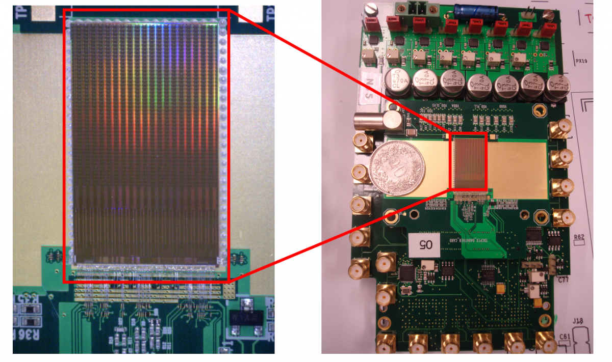
TDCPix Wire Bonded to the Test Card
The second activity is related to the support the microelectronics section is providing to the community to give access to several CMOS technologies. In 2014 a contract with TSMC for their 130 and 65 nm CMOS technologies has been put in place and the former contract with IBM for their 250 and 130 nm CMOS technologies has been transferred to MOSIS (as you might have heard, IBM sold their foundries to Global Foundry). The design kits for these technologies have been developed under ESE supervision and training courses for the community have been organised. In addition the group either participated in or conducted extensive radiation qualification campaigns. This service work (as well as the work done for the electronics pool or for the power supplies and crates delivery and maintenance) is not done under the spotlights but is of primary importance for the experiments.
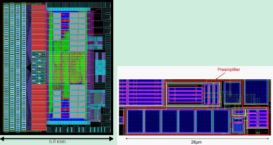
View of a 256-channel silicon strip readout ASIC in 130 nm CMOS technology (left) and of a preamplifier in 65 nm CMOS technology (right)
The third activity is related to the so-called “white-paper projects” which were launched in 2008. ESE was in charge of IC technologies and common building blocks (WP1), On-detector power distribution (WP2) and Radiation hard optical link (WP3). The WP2 objective was the delivery of a radiation hard and magnetic field tolerant DC-DC converter while WP3 was in charge of delivering a radiation hard 4.8 Gbps bidirectional optical link. Both projects entered in a production phase in 2014. The latest version of the DC-DC converter is based on the FEAST2 ASIC (see http://project-dcdc.web.cern.ch/project-dcdc/Default.html). About 3500 full converters have been delivered to date as well as 2500 chips for those willing to design their own converter module. In the framework of WP3 (see https://espace.cern.ch/GBT-Project/GBTX/Specifications/Forms/AllItems.aspx) a set of chips (the GBT chipset consists of a 4.8 Gbps serialiser-deserialiser [GBTX], a laser driver [GBLD], a transimpedance amplifier [GBTIA] and a Slow Control Adaptor [GBT-SCA]) has been designed as well as two optical modules: a transceiver (VTRx) and a dual transmitter (VTTx). The production process has started and will expand over 2015 and a part of 2016 to deliver more than 50000 GBTX and about 10000 VTRx and 20000 VTTx.
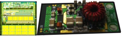
View of the 2.7 x 2.9 mm2 AMIS5 prototype ASIC(left) and of a complete converter module (13 x 28 mm2), including the air-core inductor (right)
In 2015, ESE will pursue its strong involvement in the upgrades of the LHC experiments and consolidate the readout electronics delivered to NA62. An effort in view of facilitating the sharing of designs among chip designers (IP blocks) will be launched. Several projects will continue (e.g. new TTC system, infrastructure for xTCA systems) or be launched (low power GBT, new versatile links) in view of HL-LHC.