![]()
64 channel picosecond time resolution instrumentation in 25 milligrams of silicon
The EP-ESE group has finalized the development of a 64 channel picosecond TDC (Time to Digital Converter) ASIC and 20 thousand pieces have been produced. One of the key challenges for future HEP experiments is the development of very high time resolution detectors and systems, as this can result in improved performance of TOF (Time of Flight) detectors, trackers, calorimeters and other systems. The need for compactness and extreme time precision motivated the design and development of the PicoTDC that bridges the gap between developments on fast timing detectors and currently available TDCs. It is a highly improved TDC made as a continuation of the 15 years old HPTDC chip, which has been extensively used in the LHC experiments but also by experiments in other laboratories as well as by commercial companies.
The PicoTDC development started as a PhD project to find the best time measurement circuit architecture and prototype activities together with the development of a highly stable PLL circuit by a PHD student from Leuven university. It was followed by a four-year development of the complete high-rate 64channel TDC in 65nm CMOS technology, with a highly flexible data buffering and processing architecture to enable its use in a large set of different detectors and systems. Two years of extended testing and characterization of the final chip followed, stretched by nearly two years of unfortunate delays to get production chips packaged, caused by the ASIC crisis that has put severe stress on the ASIC and packaging industry in the last year(s). Currently the production test for the 20k chips is being finalized at CERN.
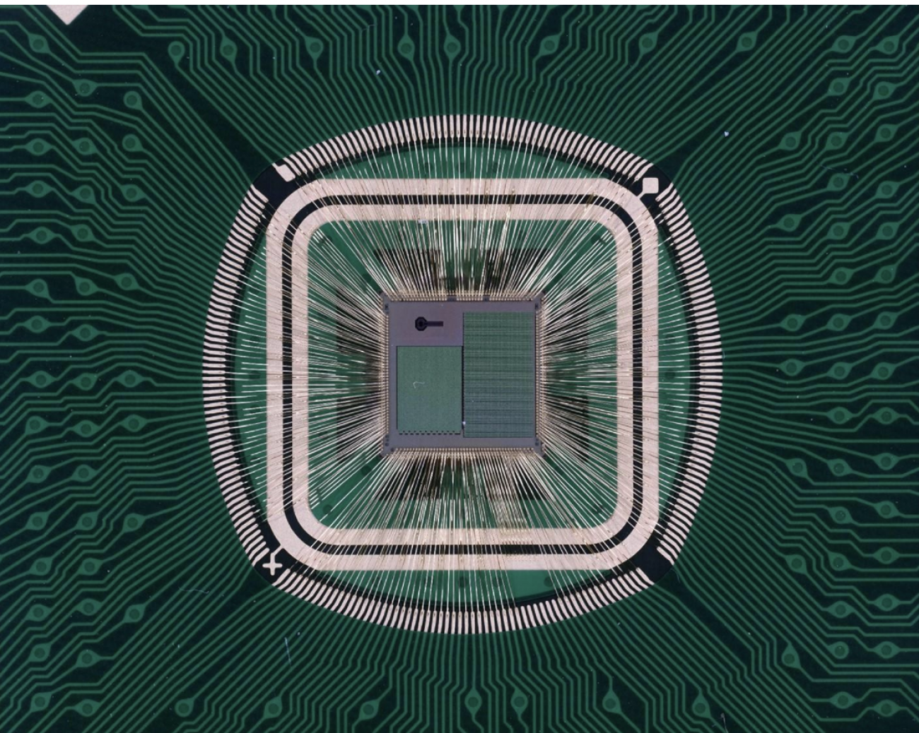
Naked 25 milligram PicoTDC on testing card.
The PicoTDC architecture (see image below) allows flexible time measurements of high rate signal transitions and pulse widths, followed by extensive data buffering and optional trigger selection time windows with programmable latency, width and when needed also overlapping time windows.
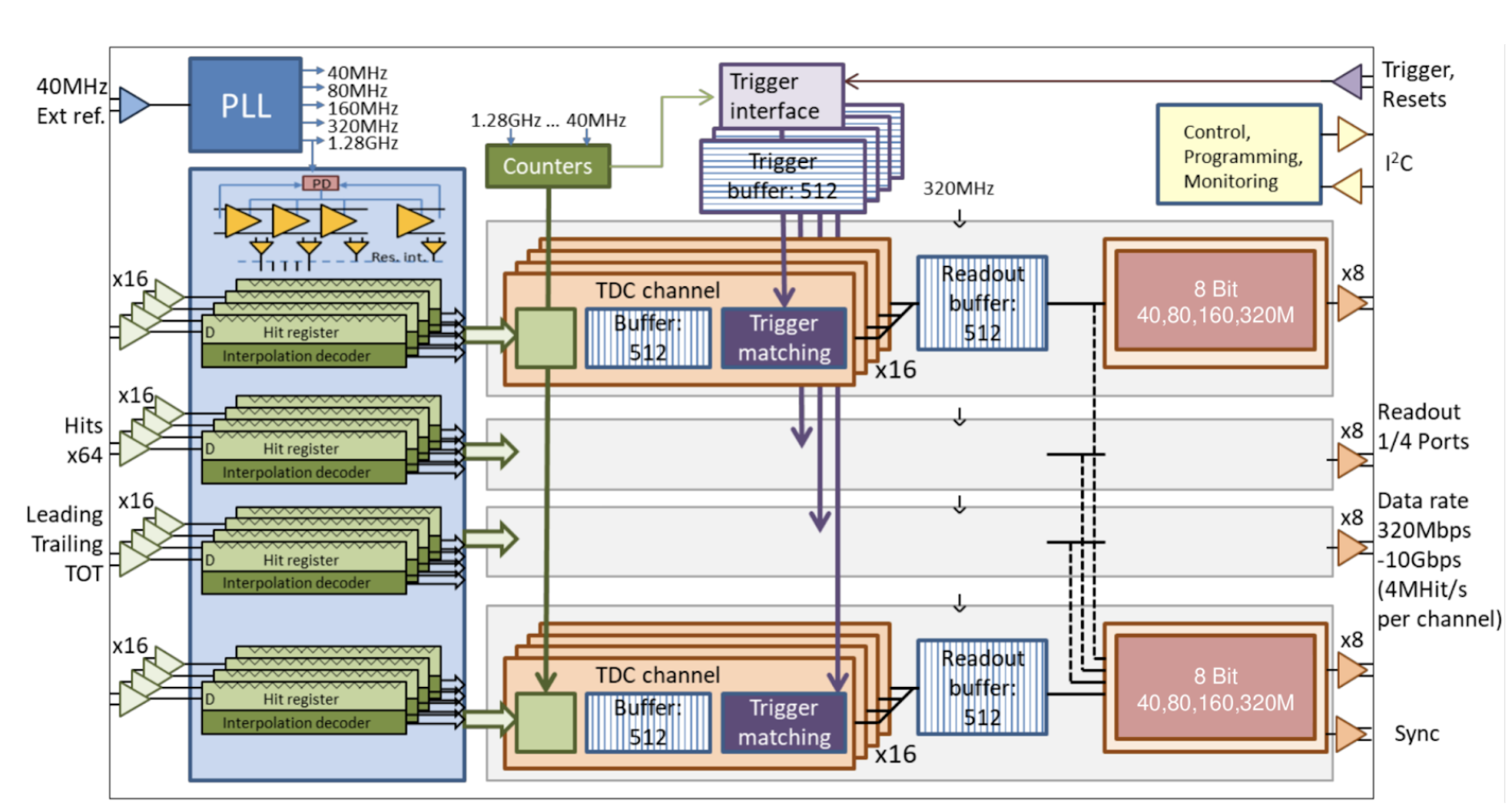
PicoTDC architecture with flexible data buffering, optional triggered event data selection and readout interface.
Timing performance across all channels has been measured to be 3-4ps RMS, without any particular time calibration or corrections applied. If timing calibration is combined with simple offline corrections, effective time resolution and precision as good as 1-2ps RMS can be obtained as shown in the two plots below.
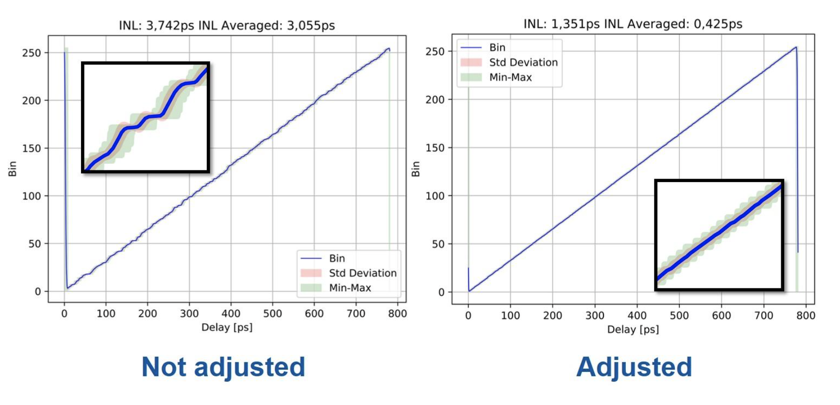
Measured Time sweep performance, un-adjusted and adjusted, with effective INL RMS resolution of 3.7ps and 1.4 ps covering 780ps (full chip dynamic range is 200us).
A large number (~30) of HEP groups are in the process of evaluating the use of the PicoTDC for detector upgrades or new experiments, taking advantage of high precision time measurements on hundreds or thousands of channels. Moreover, the high-performance of the chip allows for applications beyond HEP that require precise time-tagging of electronic signals, e.g. for electron and photon detection in medical imaging, laser ranging, life science, material research or scientific instrumentation.
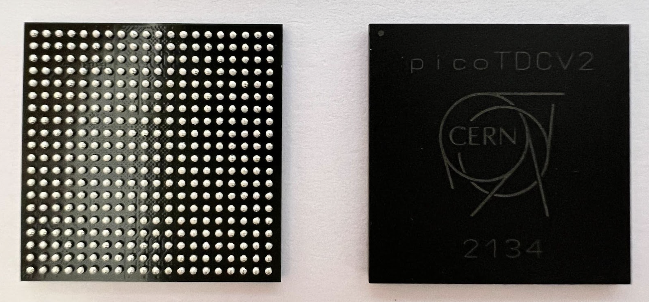
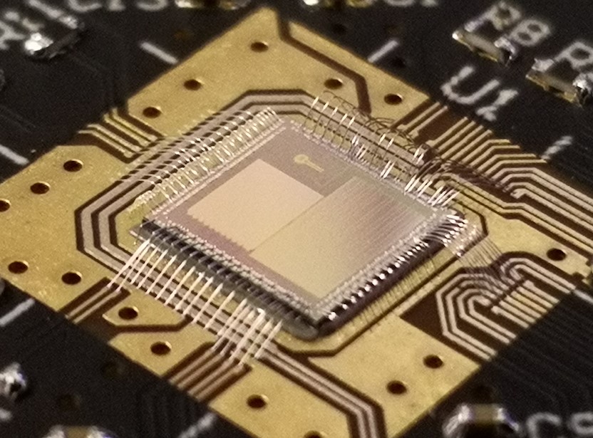
PicoTDC chip in final 400 pin ball grid array package.
A small evaluation board, together with a commercial FPGA board with available firmware and software, allow users to get an easy start to use the PicoTDC. Several companies, having signed CERN knowledge and technology transfer contracts, are actively developing instrumentation and systems based on the new PicoTDC.
Detailed info on the PicoTDC can be found in TWEPP 2019 presentation: HERE
Detailed manuals, etc. are available on dedicated sharepoint site: https://espace.cern.ch/PicoTDC
(requires access to be granted via PicoTDC users Egroup: PicoTDC@cern.ch).