![]()
Building a Microelectronics Foundation for Tomorrow’s Detectors
The challenge: smarter chips in harsher places
Particle physics detectors have always pushed electronics to their limits. The next generation of tracking systems and calorimeters will depend critically on dense, intelligent, low power and radiation-hard microelectronics: front-end ASICs that can survive for decades in harsh environments, having their own power regulation, and even perform on-detector data processing.
These are precisely the kinds of technologies being developed within Work Package 5 (WP5) of the EP R&D programme, which focuses on integrated-circuit technologies and interconnects. Now in its second phase, WP5 builds on the achievements of the initial programme while expanding its scope.
WP5 is organised around five interlocking activities: qualifying a modern deep-submicron CMOS process for the radiation environments of HEP experiments; developing a shared library of reusable analogue and mixed-signal IP blocks; building an automated, radiation-aware SoC generation framework; developing efficient on-chip and near-chip power converters; and exploring 3D interconnect technologies that will reshape how readout chips are assembled and packaged. Together, these efforts aim to make state-of-the-art microelectronics more accessible to the HEP community and to lay the groundwork for upcoming experimental upgrades and future projects.
Qualifying the technology: 28 nm CMOS as a community standard
As front-end electronics for future detectors become more complex and compact, there is growing pressure to move to deep-submicron CMOS technologies. Among them, 28 nm is particularly attractive: it offers high digital density, low power consumption and access to industrial design ecosystems. For high-energy physics, however, such technologies cannot simply be “taken off the shelf”. They must first be understood and qualified for the harsh operating conditions of present and future experiments. Within the EP R&D programme, this work is carried out through WP5.1, dedicated to technology evaluation, and WP5.2, focused on IP blocks, which together are turning a commercial 28 nm process into a well-characterised platform for radiation-tolerant ASIC design.
The focus of WP5.1 is on mapping out how 28 nm devices behave under ionising radiation, and in particular how this behavior depends on the rate at which the dose is delivered. To this end, the team used the EXP28:TID test chip [1], designed and fabricated in 2023, which hosts SRAM arrays and ring oscillators laid out in representative configurations. Irradiation campaigns performed at CERN using X-rays revealed a clear and somewhat counter-intuitive trend: devices exposed at low dose rate showed a larger increase in leakage current than those subjected to a rapid “high-dose-rate” exposure reaching the same total dose. This sensitivity to true dose-rate effects is a crucial ingredient for long-term reliability studies, since detectors accumulate radiation over many years rather than in short bursts.
To better understand the underlying mechanisms and to find ways of accelerating qualification, the group carried out complementary tests on isolated transistors at elevated temperature. Elevated temperature irradiation is a technique used to evaluate the presence of ELDRS (enhanced Low-Dose-Rate sensitivity) in electronic components through high-dose-rate tests. The comparison between room-temperature and high-temperature irradiations suggests that, for this technology, running at a higher temperature may mimic the damage that would otherwise build up slowly at a low dose rate. If validated more broadly, this approach could considerably speed up the qualification of new ASICs: instead of waiting months to reach an equivalent lifetime dose at a realistic rate, designers could use shorter high-temperature campaigns to predict the degradation expected over a decade of operation in an experiment. The importance of these findings was recognised with a dedicated contribution to RADECS 2024 and the publication “ELDRS in a Commercial 28 nm CMOS Technology” in IEEE Transactions on Nuclear Science [1].
A second finding emerged as something of a surprise. Reverse-biased p–n junctions — the most basic building block in CMOS — develop unexpectedly high leakage currents under total ionising does (TID) when voltage differences exceed a few volts. In practice, this means that radiation can make small unwanted currents appear in parts of a chip that are normally expected to show negligible leakage. This effect was traced as the root cause of a transient malfunction in a DC–DC converter prototype and anomalous behaviour in commercial ESD protection circuitry. To isolate and map the phenomenon across different junction types, bias conditions and temperatures, a dedicated test structure was submitted in 2024. The results feed directly into layout guidelines now distributed via the CERN ASIC support website [2], and the findings were presented at RADECS 2025 [3].
Radiation effects in HEP environments are not limited to cumulative damage; single-event effects caused by hadrons are equally important. A complementary test chip, EXP28:SEE [2], has therefore been used to assess the response of SRAMs and logic circuitry to protons and neutrons. Irradiation campaigns carried out in 2023 measured single-bit upsets (SBU), multiple-bit upsets (MBU) and single-event transients (SET) in a range of circuitry configurations, providing cross-sections and error signatures that can be used to dimension redundancy and error-correction schemes. In addition, a dedicated programme of single-event latch-up (SEL) tests has been completed to establish safe operating conditions and to check whether special layout precautions are needed. All results have been consolidated into a comprehensive report published on the CERN ASIC support website [2], where they are already guiding the design of new chips for LHC experiments and EP R&D demonstrators.
Systematic irradiation campaigns with protons, neutrons, and heavy ions have characterised the susceptibility of SRAMs and logic structures to single-bit upsets, multi-bit upsets, and single-event transients. A key finding is that single-event latch-up in 28 nm CMOS occurs only under extreme conditions—triggered by the heaviest ions and at voltages well beyond realistic operating ranges—thereby confirming its suitability for mainstream use. All SEE characterisation results have been compiled into a public report on the CERN ASIC support website, providing a valuable reference for designers across collaborating institutes.
The practical result of all this work is that 28 nm bulk CMOS is now a well-understood, shared technology platform for the HEP community.
A shared IP library
In parallel with the technology evaluation, WP5.2 aims to eliminate the need for each ASIC project to repeatedly design the same core analogue and mixed-signal circuitry from scratch. The AMTest28 chip — designed in 2023 and characterised throughout 2024 — prototyped a suite of community-facing blocks: bandgap voltage references optimised for radiation tolerance, a compact TID monitoring circuit small enough to embed in any ASIC, a fast rail-to-rail operational amplifier, and an 8-bit DAC. A computer-controlled test bench was developed and distributed to collaborating institutes so that each block can be characterised consistently across sites.
As this catalogue of validated building blocks grows, the model is shifting: rather than developing everything in-house, WP5.2 is evolving into a curated shared repository. Community institutes contribute their own IP blocks; a centrally managed library — hosted at asicsupport.web.cern.ch — provides controlled access and a common quality baseline. A 12-bit, 2 MS/s, 16-channel monitoring ADC — a block required in virtually every complex ASIC — is being developed in close collaboration with a specialist company, with CERN engineers enforcing radiation-hardening guidelines throughout. The aim is for IP blocks to be instantiated with the same confidence one gives standard cells: tested, documented, and ready to use.
From chips to systems: the SOCRATES ecosystem
Individual IP blocks and a qualified technology are necessary but not sufficient. Building a complete, radiation-tolerant System-on-Chip from scratch for each new application is enormously expensive in engineering time, and it invites the same mistakes to be made repeatedly. The answer developed by WP5.3 (SoC Ecosystem and On-Detector Intelligence) is a framework that automates the most error-prone parts of the process. WP5.3 is trying to move HEP chip design from ad-hoc , project-by-project development towards a reusable, automated design ecosystem.
SoCMake and SOCRATES: generation, not just design
At the heart of the ecosystem is SoCMake, a CMake-based hardware/software build system that treats an SoC the way a compiler treats source code: a single architectural description drives the automatic generation of synthesisable RTL, software drivers, hardware abstraction layers, UVM testbenches with fault-injection utilities, EDA configuration files, and documentation — all in one reproducible flow [4]. SoCMake was then wrapped with radiation-tolerant IP blocks, bus protocols, and fault-tolerance tooling under the umbrella name SOCRATES (SOC Radiation Tolerant EcoSystem) [5].
The radiation-tolerant building blocks inside SOCRATES include: automatic Triple Modular Redundancy (TMR) insertion via the TMRG tool, with formal verification of correct triplication; a fault-injection framework for pre-silicon SEU simulation; and APB-RT, a custom peripheral bus derived from the industry-standard AMBA APB5 protocol, which adds Hamming(13,8) SECDED encoding on data and address lines and triplicated control signals. The combination reduces the number of individual bus wires by 66% compared to full triplication, saving routing resources and power while still enabling robust error correction [5].
The philosophy is deliberate: rather than a fixed SoC architecture, SOCRATES is a generator. It supports multiple open-source RISC-V processor cores (Ibex, VeeR EL2, SCR1, PicoRV32), standard interconnects (AMBA AXI4, OBI), and any peripheral IP block that conforms to the APB-RT interface. Assembling a new SoC variant for a different application — say, an embedded controller for a pixel detector — becomes an exercise in selecting and connecting components, not in re-engineering from first principles.
TriglaV: the proof in silicon
Any framework is only as convincing as its silicon. To validate the complete SOCRATES flow end-to-end, the team designed TriglaV: a 32-bit RISC-V-based fault-tolerant microcontroller SoC fabricated in 28 nm bulk CMOS, submitted at the end of 2024 on a multi-project wafer alongside designs from the technology-evaluation and powering activities.
TriglaV integrates a fully triplicated Ibex RV32IMC core (incurring a 4× area overhead over the un-hardened core, but providing single-cycle SEU self-correction via majority voters at every flip-flop), 64 kB of on-chip SRAM protected by Hamming(13,8) ECC and continuously scrubbed by a dedicated Memory Scrubbing and Protection Unit, a triplicated OBI multi-master crossbar, and standard peripherals — UART, GPIO, timers, PLIC, I²C — all hanging off the APB-RT bus. TMR flip-flops belonging to the same redundancy set are physically separated by at least 10 μm in the layout to suppress multi-cell upsets from a single particle strike.
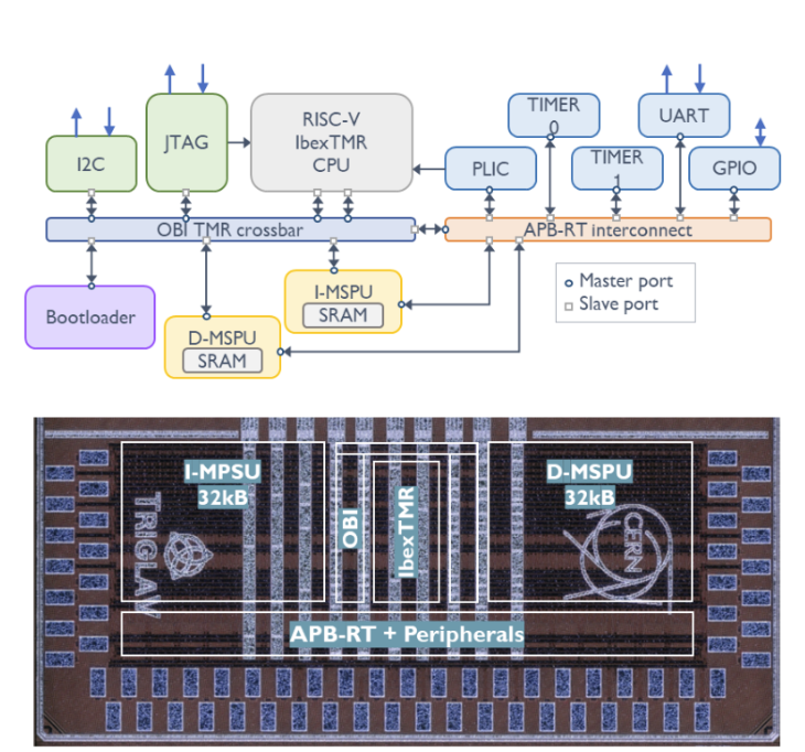
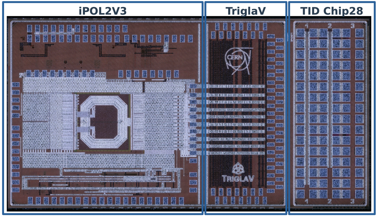
Figure 1. TriglaV architecture (top) and die microscope photograph (bottom) of the 1.6 mm² chip in 28 nm bulk CMOS. The triplicated IbexTMR processor, two 32 kB scrubbing memory units (I-MSPU and D-MSPU), the OBI crossbar, and the APB-RT peripheral ring are all visible on the annotated die image.
The experimental results validated both the chip and the flow that produced it. At nominal operating conditions (0.9 V, 250 MHz), TriglaV draws approximately 69 mW — a realistic reference for future radiation-tolerant SoC designs. X-ray irradiation at CERN to 1 Grad TID showed full functionality across all tested voltages and clock frequencies up to 300 MHz, with only the expected increase in leakage current [6]. Heavy-ion testing at UCLouvain (LET range 3.2– 61.3 MeV·cm²/mg) demonstrated that TMR and ECC together correct the vast majority of upsets, with per-bit SEU cross-sections consistent with previously published 28 nm data [6].
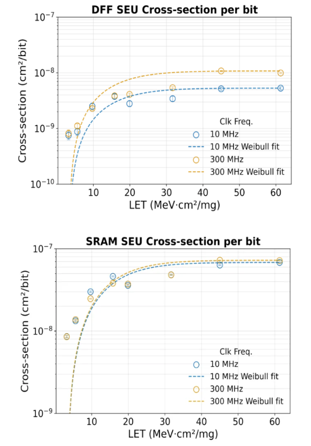
Figure 2. SEU cross-sections measured in TriglaV with TMR correction counters (left, flip-flops) and ECC counters (right, SRAM) during heavy-ion irradiation at UCLouvain. Data shown for 10 MHz and 300 MHz clock frequencies; dashed lines are Weibull fits. Both are consistent with baseline 28 nm technology data.
A small number of Single-Event Functional Interrupts (SEFIs) were recorded during benchmark execution, and their root causes have been identified: un-hardened foundry SRAM macros, residual layout-level Single-Event Multi-Transients, and an I/O reset-sensitivity. These are known quantities with clear remediation paths. Even conservatively, the estimated SEFI rate for HL-LHC inner-tracker conditions is below one per hour — and far lower for most realistic applications. The take-home message is clear: TriglaV has shown in silicon that the SOCRATES approach can deliver complex, radiation-tolerant on-detector intelligence in 28 nm CMOS.
PixESL: understanding the system before you build it
Silicon prototypes validate; virtual prototypes explore. The PixESL framework — written in industry-standard C++/SystemC — models the entire readout chain of a pixel detector, from particle interaction in the sensor to the departure of a formatted data packet from the chip. It runs tens of times faster than RTL simulation, allowing architects to sweep large design spaces and quantify the impact of architectural choices before committing to hardware [7].
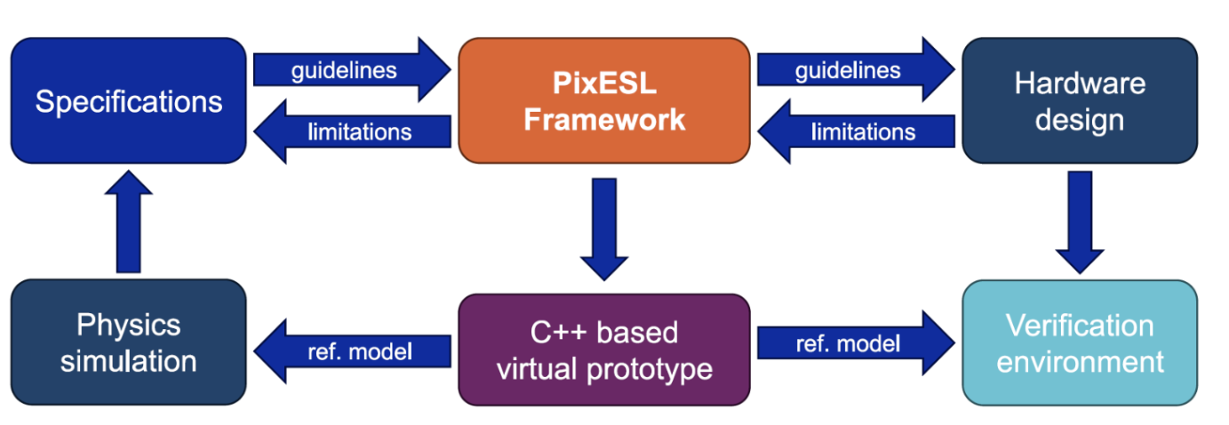
Figure 3. The PixESL virtual-prototyping framework couples physics simulation, hardware specifications, and verification environments through a common C++/SystemC virtual prototype. The same model that guides architecture choices is reused as a reference during chip verification.
The framework’s practical impact is already substantial. Simulations of the LHCb VELO-Upgrade-II detector (withinthe framework of the LA-Picopix ASIC, 256 × 384 pixels at 6.2 mm from the interaction vertex) revealed that the baseline readout architecture would saturate under the upgraded hit rates. A redesigned architecture — developed in direct response to PixESL results — improved data-readout efficiency from 86% to nearly 100% while cutting average latency by two-thirds, as shown below.
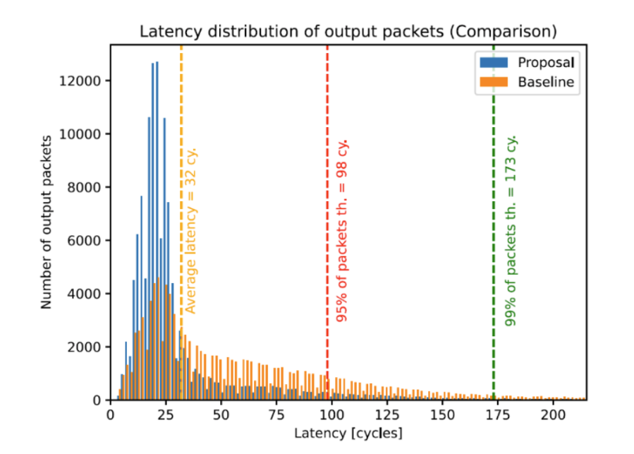
Figure 4. PixESL latency simulation for LA-Picopix/VELO-II comparing the baseline readout architecture (orange) and the proposed redesign (blue). Average latency falls from >98 cycles to 32 cycles; the long tail of the baseline distribution is eliminated entirely.
Crucially, PixESL doesn't get shelved once the design is chosen: the same virtual prototype is reused as a reference model during chip verification, ensuring that the final hardware behaves exactly as intended. PixESL is fully open-source and publicly available on CERN's GitLab, making it a shared resource for the entire High Energy Physics community, a common language between the worlds of physics simulation and electronics design that any detector project can adopt and build upon.
It has been adopted by the ALICE3 programme, is being coupled with the open source framework for SoC Virtual Prototyping developed by ETH Zurich, namely GvSOC [15] ,for end-to-end SoC-level studies, and is being interfaced with AllPix² for semiconductor-level sensor simulation [16]. All steps toward a unified simulation chain from charge deposition to on-chip data reduction. The framework received a Best Research Paper award at DVCon Europe 2024 and an Oral Presentation Award at TWEPP 2024 [8,9].
The hardware accelerator strand of WP5.3 complements PixESL by translating its architectural insights into silicon. An Event Sorter and Builder module — whose sizing was determined entirely through PixESL simulations — was implemented in 28 nm CMOS and integrated into the LA-Picopix design: it processes up to 200 Gbps at 320 MHz with less than 1% packet loss, consuming under 250 mW and under 7 mm², with fully triplicated control logic [10].
Powering the front end: from 48 V to 0.9 V on-chip
No matter how sophisticated the digital logic, a front-end ASIC is useless without reliable, efficient power delivery. In future detectors — where material budget is precious, service routing is constrained, and the electronics may be inaccessible for years — power delivery is a first-class design problem. WP5.4 (Powering Solutions) addresses the full conversion chain, from the long-haul distribution rail to the transistor gate.
bPOL48V: distributing power at 48 volts
The first challenge is getting power from counting rooms (or service areas) to detector modules efficiently. High-voltage distribution — 48 V over long cables — minimises resistive losses, but the front-end chips operate at 0.9 V. The bPOL48V module addresses the first conversion stage: a compact 55 × 24 × 3 mm² board combining a custom GaN-controller ASIC, a commercial GaN power stage, and a custom air-core PCB inductor. Its resonant architecture operates at ~150 MHz and achieves up to 94% efficiency at 12 V output with a 10 A current rating — meeting the demanding requirements of HL-LHC experiments. The module is now available to collaborating institutes and has been characterised and irradiation-tested for HEP deployment [11].
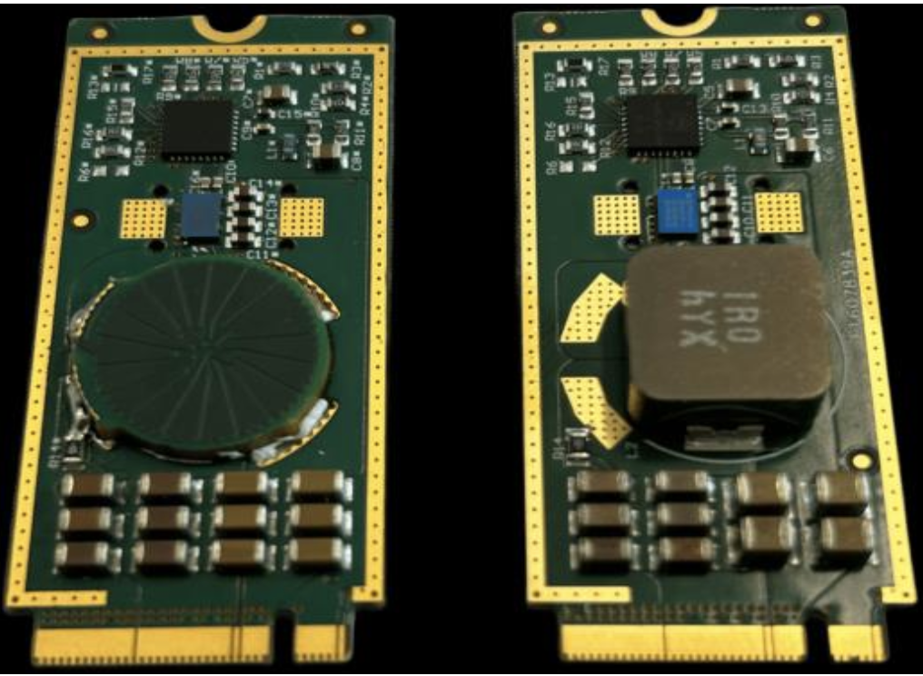
Figure 5. The bPOL48V module (both sides shown), measuring 55 × 24 × 3 mm². It steps 48 V down to 5 V or 12 V at up to 10 A with efficiencies above 90%, combining a custom GaN-controller ASIC and a custom air-core PCB inductor on a compact M.2 form-factor board.
iPOL: the converter that lives on your chip
The second and more radical step is to integrate the final-stage converter directly into the front-end ASIC — eliminating external capacitors and inductors, shrinking the power-delivery network, and reducing the sensitivity to ground bounce and supply noise. The iPOL family of Fully Integrated Voltage Regulators (FIVRs) does precisely this, using only core 28 nm transistors (0.9 V thin-oxide devices) to achieve exceptional radiation tolerance, with all passive components on-chip.
Three variants have been developed and tested:
— iPOL5V: steps 5 V down to 0.9 V at up to 400 mA, using a resonant topology at 150 MHz with up to 75% efficiency;
— iPOL2V3: steps 2.3 V down to 0.9 V at up to 200 mA — integrated with TriglaV to validate the complete system-level power architecture;
— linPOL1V2: a linear regulator from 1.2 V to 0.9 V at up to 200 mA, for low-noise applications
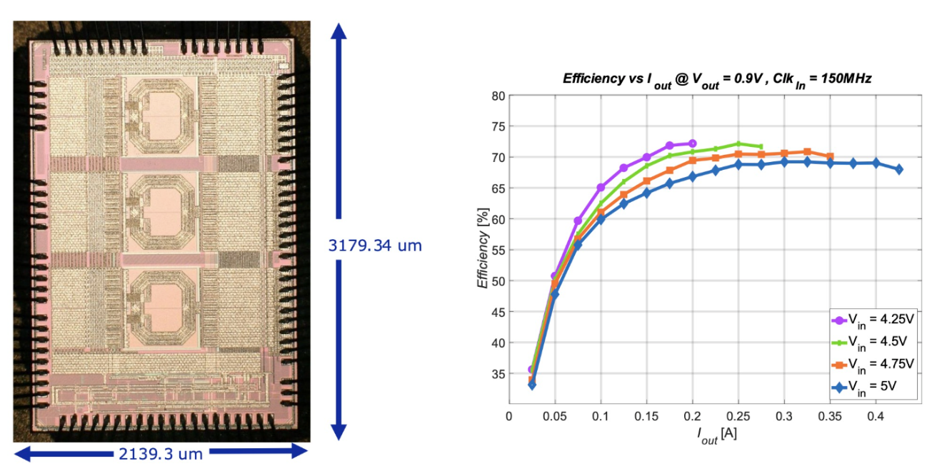
Figure 6. Die photograph of the iPOL5V converter in 28 nm CMOS (2.1 × 3.2 mm²). All passive components — inductors and capacitors — are integrated on-chip. The resonant converter operates at 150 MHz and has been radiation-tested to 1.7 Grad TID with no significant performance degradation.
All three ASICs have been irradiation-tested to 1.7 Grad TID and with heavy ions up to 48 MeV/(mg/cm²) with no significant performance degradation [12]. An unexpected TID-induced leakage path in iPOL5V, identified during 2024 characterisation, was fully understood, corrected, and translated into updated layout guidelines — an example of how the WP5 feedback loop from characterisation to design rules works in practice. The system-level integration of iPOL2V3 with TriglaV — a complete, powered, radiation-tolerant SoC from a single 28 nm wafer run — is a concrete demonstration that the pieces fit together.
3D interconnects: rethinking how chips connect to the world
Even the most sophisticated ASIC is limited by how it interfaces to the rest of the detector module. Traditional wire-bonding — thin wires looping from the chip edge to the carrier board — imposes dead area at every edge, introduces parasitic inductance and capacitance to the detriment of signal and power integrity, and prevents chips from being butted on four sides. For future pixel detectors aiming for high data-throughput, minimal dead area and maximum channel density, these are severe constraints.
WP5.5 (3D Interconnects and Advanced Packaging) is studyingThrough-Silicon Via (TSV) technology as the alternative. TSVs route signals vertically through the silicon itself, from the active front side to a redistribution layer (RDL) on the back side, where solder balls can connect to a carrier substrate just like a ball-grid array. With no wire-bond pads required at the chip edges, the active area can extend to all four sides — enabling truly seamless, tiled detector modules with short, low-loss interconnections.
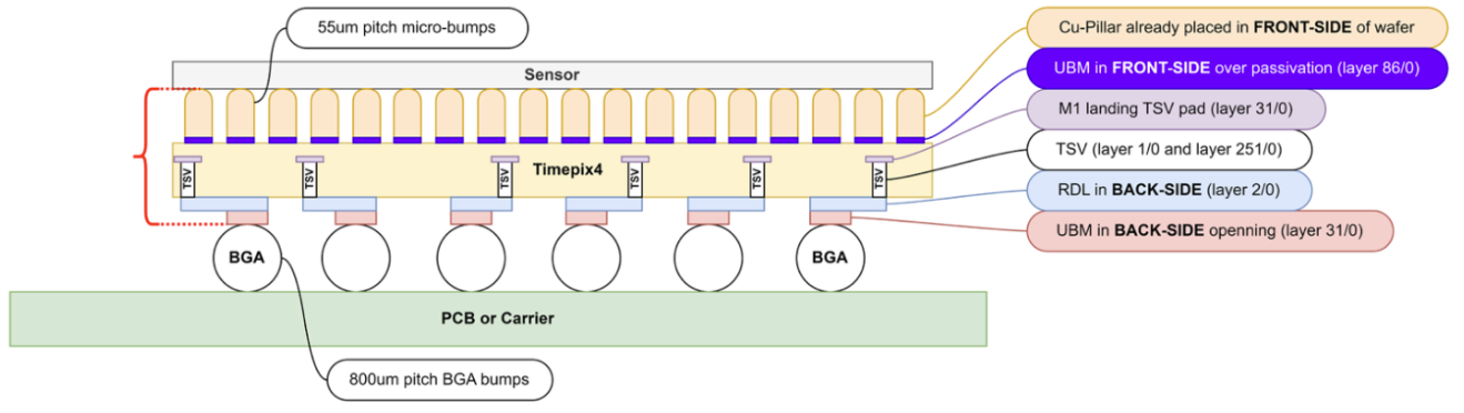
Figure 7. Conceptual diagram illustrating the use of the Timepix4 ASIC for feasibility studies of 3D stacking.
The Timepix4 chip, which already includes the layout features needed for TSV post-processing, serves as the primary test vehicle. Working with four industrial vendors spanning 200 mm and 300 mm wafer formats — two European suppliers already delivering processed wafers, a third European vendor under discussion, and a top-10 global OSAT company whose 300 mm pilot run delivered 100% TSV yield in mid-2025 — WP5.5 is methodically building both the technical knowledge and the supply chain for future ASIC assemblies [13].
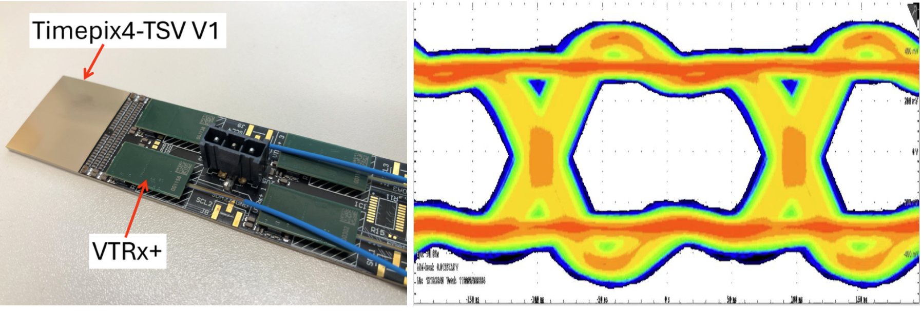
Figure 8. Left: opto-demonstrator module, showing aTimepix4-TSV interconnected with four VTRx+ modules. Right: eye diagram produced with a pseudo-random bit sequence using one of the 16 channels, through TSV and optical fiber at 5.12Gbps.
System demonstrators have advanced in parallel. A Timepix4 chip with TSV processing was successfully bump-bonded to a silicon pixel sensor and tested using a Strontium-90 radioactive source, demonstrating electrical integrity throughout the assembly. A finger-module PCB connected TSV-processed Timepix4 chips to VTRx+ optical transceivers, achieving 5.12Gbps data transmission through the full TSV-and-PCB chain while demonstrating four-side buttability potential. Working together with WP6, a proof-of-principle 3D integration module combining TSV-processed Timepix4 with a silicon-photonics device (SystemPIC) successfully transmitted data at 5.12 Gbps. . Signal and power integrity studies — evolving from simplified analytical models to full electromagnetic simulations combining ASIC and substrate layouts— are providing the co-design guidelines that future ASIC and substrate teams will need.
A platform, not a project
Viewed as a whole, WP5 is not five parallel research lines that happen to share a name. It is a deliberate effort to build a shared microelectronics platform for the HEP community: a 28nm bulk CMOS technology with documented radiation behaviour, a library of validated building blocks, automated tooling that assembles those blocks into complete SoCs, power converters that sit on the same die as the logic they supply, and packaging technologies that free future detector modules from the constraints of wire-bonding.
Each activity reinforces the others in a tightly coupled workflow. The radiation characterisation of silicon technologies in WP5.1 guides the IP library designers in WP5.2, using suitable technologies and identifying which device structures are robust or vulnerable. The IP blocks developed in WP5.2 then feed into the SOCRATES ecosystem in WP5.3. There, virtual prototyping enables system designers to efficiently explore large design spaces and assess the impact of architectural choices before committing to hardware design.
In parallel, the iPOL converters from WP5.4 are implemented in the selected technology—28 nm CMOS in this demonstrator—and integrated within the TriglaV SoC developed in WP5.3. Finally, the TSV interconnect R&D in WP5.5 uses Timepix4 as a test vehicle to evaluate processes from multiple vendors. These results will ultimately support 3D integration in future detector upgrades, building on the silicon technologies and IP blocks developed across the other work packages.
The immediate next steps are already defined. SOCRATES and SoCMake will be used to design an embedded microcontroller IP block for LA-PicoPix — a pixel detector readout ASIC currently in 28 nm development — providing programmable monitoring, calibration, and control on-chip that would previously have relied entirely on fixed-function logic. A new initiative, DRIVE (Data-Driven Readout for Intelligent and Versatile Electronics), will explore SoC-based programmable periphery for data-driven, intelligent pixel-array readout. PixESL will deepen its coupling to physics simulation and SoC-level modelling, moving toward the unified simulation chain from sensor charge deposition to on-chip data reduction that the community has long needed.
On the technology side, further characterisation of the 28 nm process — especially the dose-rate and pn-junction leakage effects now under study — will refine design rules and expand the community’s confidence in using this node for ambitious new projects. And on the packaging side, WP5.5 will intensify its TSV vendor evaluations, with the LA-PicoPix ASIC — which integrates multi-gigabit transmitters developed within WP6and will itself be a SOCRATES-hosted SoC — as the first real target for production-quality 3D integration.
The physics ambitions of the HEP community have always outpaced the electronics available to realise them. The purpose of WP5 is to close that gap — by carefully and collaboratively building the microelectronics infrastructure that the next generation of experiments will take for granted.
Cover photo: Timepix4 die in Test Socket. Cupillar bumps on the top side. Source: CERN Experimental Physics Department. EP Department Annual Report 2025. CERN, 2025. Available at: https://cds.cern.ch/record/2955137/files/ep_annual_report_2025.pdf?version=1
References
- G. Borghello et al., “ELDRS in a commercial 28 nm CMOS technology,” IEEE Trans. Nucl. Sci. 72 (2025) 2276–2285. DOI: 10.1109/TNS.2025.3543658
- CERN ASIC Support and Foundry Service: https://asicsupport.web.cern.ch
- K. Sarbandi et al., “TID-induced leakage current in a commercial 28-nm CMOS technology,” RADECS 2025, Sept. 2025.
- R. Pejašinović et al., “Hardware and software build flow with SoCMake,” WOSET 2024.
- M. Andorno et al., “SOCRATES: a radiation-tolerant SoC generator framework,” JINST 20 C02017 (2025). DOI: 10.1088/1748-0221/20/02/C02017
- N. Anvesh et al., “Design and Evaluation of TriglaV: A Prototype SoC ASIC for Particle Physics Applications realised with the SOCRATES Platform,” TWEPP 2025, Rethymno, Greece.
- F. E. Brambilla et al., “SystemC framework for architecture modelling of electronic systems in future particle detectors,” JINST 19.01 C01039 (2024). DOI: 10.1088/1748-0221/19/01/C01039
- F. E. Brambilla et al., “Virtual Prototyping Framework for Pixel Detector Electronics in High Energy Physics,” DVCon Europe 2024 (Best Research Paper award). DOI: 10.30420/566438001
- J. Dhaliwal et al., “Applications of PixESL framework on pixel detectors for High Energy Physics experiments,” TWEPP 2024 (Oral Presentation Award).
- “On-Chip Packets Sorting for High-Throughput Data-Driven Pixel Detectors in a 28 nm CMOS Technology,” TWEPP 2025. https://indico.cern.ch/event/1502285/contributions/6554447/
- N. H. Van der Blij et al., “Optimized rad-hard DC/DC converters for HEP applications,” JINST 19.12 C12018 (2024). DOI: 10.1088/1748-0221/19/12/C12018
- G. Bantemits et al., “Next generation fully integrated DCDC converters for HEP applications in 28 nm technology,” TWEPP 2024 (Oral Presentation Award).
- F. P. Diaz et al., “3D integration of pixel readout chips using Through-Silicon-Vias,” JINST 20.01 C01017 (2025). DOI: 10.1088/1748-0221/20/01/C01017
- PixESL open-source framework: https://gitlab.cern.ch/iod/pixesl-group
- GvSOC open-source framework: https://github.com/gvsoc/gvsoc
- AllPix2 framework: https://allpix-squared.docs.cern.ch/