![]()
Development of Radiation Tolerant Silicon Detectors for the LHC and HL-LHC
Introduction
The potential of semiconductor-based detectors for particle detection in nuclear and high-energy physics (HEP) has been identified as early as 1960. However, it took two more decades of development to transform these detectors into reliable, fully operational systems. Silicon-based tracking detectors made their debut in HEP experiments during the 1980s, revolutionizing the field with their unmatched spatial resolution and high-rate capabilities. This breakthrough established them as the preferred technology for particle tracking in HEP experiments, a role they continue to dominate today. As collider luminosity increased, a critical challenge emerged: radiation damage caused by the intense flux of particles and photons passing through these detectors.
Silicon detector properties and their usage in HEP
Silicon sensors are lightweight, mechanically stable, and self-supporting, enabling fast charge transport with collection times under 20 ns in a 300 μm device. This speed accommodates particle interaction rates such as 40 MHz at the LHC. Their high ionization density provides excellent signal-to-noise ratios with thin sensor layers. The introduction of the planar detector process in 1980 was transformative, using photolithographic techniques to achieve micron-level resolution. This also spurred advancements in readout electronics, culminating in integrated devices that combine sensors and electronics. Figure 1 illustrates the growth in silicon detector use over 60 years, reflecting their importance in HEP.
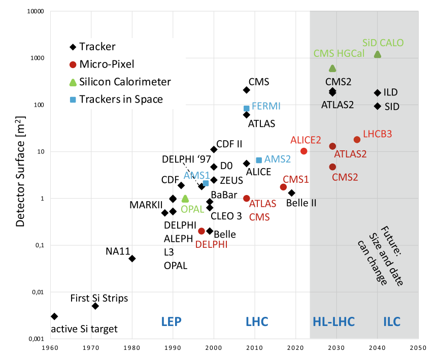
Figure 1: Evolution of silicon detector area. In logarithmic scale, the plot displays the increase in area over the last 60 years, including as well the detectors approved and considered for the next decades (taken from [1]).
Radiation damage challenges for the long-term operation
As accelerators became more powerful, detectors were placed closer to interaction points to maximize particle interaction rates. This proximity significantly enhanced data collection but also subjected detectors to increasingly intense radiation levels, accelerating their ageing and causing damage. For example, the inner pixel detectors at the High Luminosity LHC (HL-LHC) are expected to endure a particle of some 1016 highly damaging particles per cm2 and a dose of about 10 MGy. These extreme conditions present formidable challenges to detector performance and longevity.
To address this, the HEP community initiated extensive R&D programs to study radiation damage mechanisms and develop innovative mitigation strategies. These efforts aimed to ensure reliable detector performance in high-radiation environments, safeguarding the progress of particle physics in the years to come.
CERN centred R&D collaborations focussing on silicon detector developments
The need for radiation-tolerant detectors emerged in the late 1980s during planning for new proton supercolliders, leading CERN to launch the RD2 project in 1990 as the first organized effort in this area. Subsequent projects, RD48 and RD50, expanded on RD2's work, with RD48 focusing on early LHC experiments and RD50 addressing long-term solutions and upgrades, particularly for the High Luminosity LHC (HL-LHC). These collaborations brought together institutions ranging from LHC experiment teams to experts in solid-state physics, materials science, and electronics, led by co-spokespersons overseeing research lines dedicated to various aspects of detector development.
The R&D efforts, funded primarily by national agencies and supplemented by a shared common fund, focussed on three main strategies to mitigate radiation damage: material engineering to enhance bulk properties, device engineering to develop innovative sensor designs, and optimizing operational conditions, such as using cryogenic temperatures to reduce damage. These strategies rely on comprehensive studies of detector physics and radiation damage mechanisms, supported by defect modelling, simulations, testing, and specialized tools.
Collaboration Focus
The efforts highlight a structured, multidisciplinary approach to addressing the technical demands of modern HEP experiments. From 1990 to 2020, the RD2, RD48, and RD50 collaborations spearheaded a series of groundbreaking advancements in radiation-tolerant silicon detectors. While the examples presented here cannot comprehensively capture three decades of multidisciplinary effort, they illustrate the breadth and depth of these achievements, shaping the future of particle physics experiments.
1.1 Characterization and parameterization of radiation damage to detectors
The journey began with efforts to understand and quantify the effects of radiation on semiconductor detectors. High-energy particles interacting with silicon detectors cause Ionizing Energy Loss (IEL) and Non-Ionizing Energy Loss (NIEL). While IEL generates the signals used for particle detection, NIEL displaces atoms in the silicon lattice, creating defects that degrade detector performance. The adoption of the NIEL hypothesis provided a framework to predict radiation damage, scaling the effects of complex radiation fields to an equivalent fluence of 1 MeV neutrons.
The establishment of comprehensive NIEL functions was therefore one of the first activities when the LHC targeted RD projects started their work in 1995. In the following years, it was demonstrated that NIEL scales well for the leakage current, but has severe shortcomings in describing the change of detector depletion voltage. The work on damage characterization was throughout the first decade mainly performed on simple n-type FZ silicon pad detectors of typically 300 microns thickness, an area in the order of 0.25 cm2 and realized either (in the beginning) as Schottky diodes or (later) as devices with diffused or implanted electrodes. The detector degradation in terms of increase of leakage current, loss of charge collection efficiency and change of the full depletion voltage as a function of particle fluence, particle type and annealing time and temperature was studied in detail. Major findings were the type-inversion of the effective doping and, very unexpectedly, the increase of depletion voltage during the long-term storage at room temperature after irradiation, the so-called “reverse annealing” (1992). These insights underpinned robust models like the "Hamburg model," enabling accurate performance predictions under LHC conditions.
1.2 Defect and Material Engineering
Based on promising radiation damage studies on sensors produced from epitaxially grown silicon a wide range of silicon material engineering approaches was studied by the RD48 collaboration from 1996 onwards. The RD48 collaboration explored a wide range of silicon material engineering approaches to improve radiation tolerance in detectors. A major breakthrough was the discovery that silicon with high oxygen content exhibited improved resistance to radiation damage from charged hadrons, leading to the development of Diffusion Oxygenated FZ (DOFZ) silicon. This material reduced the increase in depletion voltage under proton and pion irradiation, though no significant improvement was observed for neutron irradiation—a phenomenon later explained as the "proton-neutron puzzle." Since 2010, oxygen-enriched FZ silicon has been used in LHC pixel detectors, which endure the highest radiation levels near the interaction points.
Advances also included the transition from n-type to p-type silicon and carbon-enriched layers in LGADs. Alternative materials like diamond found niche applications, while SiC and GaN showed potential for future research. Renewed interest in SiC and GaN emerged in 2018 with the availability of higher-quality wafers, spurring further research within the RD50 collaboration.
1.3 The microscopic origin of radiation damage – Defect characterization and modelling
Radiation damage in silicon detectors arises from particles displacing crystal atoms, creating vacancies and defects in the lattice. These defects, which can involve only silicon atoms or include impurities like oxygen or carbon, form due to temperature- and time-dependent processes, sometimes taking years to stabilize. These crystal defects introduce energy levels within the semiconductor's bandgap, altering its electrical behavior. Their effects are described by Shockley-Read-Hall statistics, which rely on precise knowledge of defect properties such as concentrations, energy levels, and carrier capture cross-sections. Techniques like Deep Level Transient Spectroscopy (DLTS) and Thermally Stimulated Current (TSC) have been instrumental in studying these defects, particularly in highly irradiated devices.
In high-energy physics, systematic studies of radiation-induced defects have yielded significant insights, many pioneered by RD48 since 1995. Key discoveries include resolving the proton-neutron puzzle with donor levels explaining space charge differences, identifying acceptor levels behind reverse annealing, and understanding leakage current increases caused by defects like trivacancy. Recent studies within the RD50 collaboration have also shed light on the boron-oxygen defect's role in acceptor removal. Over three decades, this research has produced a detailed catalogue of defect levels, enabling advanced numerical modelling and improving the design of silicon sensors for radiation-hard applications.
1.4 Device Engineering
Innovation in silicon sensor technology often begins with individual ideas or expert discussions but evolves into fully operational concepts through collaborative community efforts. Progress in this field relies on a deep understanding of the physics of device operation and the mechanisms of radiation damage, which must be mitigated to achieve high performance in the challenging environments of high-energy physics (HEP) experiments. The RD collaborations, particularly at CERN, have been instrumental in fostering the innovation and development necessary to advance sensor technology.
One of the most impactful engineering advancements has been the shift from n-type to p-type silicon bulk material for sensors. This change also involves a transition in the implant type for readout electrodes, from p-type to n-type, resulting in a switch from collecting electrons to collecting holes. While current LHC sensors made of n-type silicon are not suited for the radiation levels of the High Luminosity LHC (HL-LHC), the next-generation sensors, spanning over 1000 m², will use p-type silicon.
This paradigm shift, driven by the CERN RD50 collaboration, offers greater radiation hardness and reduced production costs for pixel devices. However, it required two decades of development, including advances in surface isolation techniques, high voltage stability, thickness optimization, and radiation hardness characterization.

Figure 2: Schematic representations of the three technology developments described in the text: (a,b) p-in-n and n-in-p strip sensors, (c) 3D sensors and (d) LGAD sensors (figures taken from [2, 3]).
3D sensors can be regarded as the most sophisticated device engineering approach. First proposed in 1997, they represent a groundbreaking innovation in detector design. Their unique structure features columnar electrodes etched perpendicularly to the wafer surface, which fundamentally redefines the relationship between the active thickness of the device and the distance charge carriers must travel to the electrodes. This geometry allows for rapid charge collection, reduced charge trapping, and operation at significantly lower voltages, making 3D sensors inherently resistant to radiation damage. However, their sophistication comes with challenges, including higher noise due to increased capacitance, small dead regions near the electrodes, and greater production costs.
The RD50 collaboration, alongside foundries at CNM in Barcelona and FBK in Trento, worked tirelessly to refine the technology. The ATLAS experiment gave the effort a decisive push, rigorously testing 3D sensors and integrating them into the innermost pixel layer (B-layer) of their detector between 2007 and 2014. This industrial-scale development marked a turning point, making 3D sensors the most radiation-hard silicon detectors available today, and securing their place in the High Luminosity LHC (HL-LHC) upgrades.
Low Gain Avalanche Diodes (LGADs) are the most recent device offspring of the CERN RD50 collaboration. They emerged in 2014 as an elegant solution for precision timing in high-energy physics. LGADs feature a gain layer—a thin, heavily doped p+ region beneath the n+ contact—that creates a strong electric field, enabling charge multiplication through impact ionization. This design achieves exceptional timing resolution in the tens of picoseconds, making LGADs invaluable for high-speed detection.
Inspired by early observations of charge gain in p-type strip sensors under high voltage, RD50 researchers rapidly developed LGADs into a versatile technology for high-energy physics and beyond, including nuclear physics, medical imaging, and astrophysics. Their adoption by ATLAS and CMS for HL-LHC precision timing detectors spurred advancements in gain layer engineering and segmentation, improving radiation hardness and spatial resolution. These innovations also enable advanced applications like 4D tracking, combining precise spatial and temporal measurements. The collaborative efforts of researchers and industry partners have driven LGADs from concept to operational readiness, leaving a lasting impact on particle detector technology and beyond.
1.5 Research tools
Evaluating the effects of radiation damage in detector materials requires specialized tools, many of which have been developed collaboratively within the CERN R&D community. One notable example is the Transient Current Technique (TCT), refined by the RD48 and RD50 collaborations. TCT involves generating non-equilibrium charge carriers in a biased sensor using ionizing particles, light pulses, or bias pulsing. By measuring time-resolved signals from these charge carriers, researchers gain detailed insights into sensor properties like depletion voltage, charge collection efficiency, and electric field distribution. Originating in the late 1960s, TCT gained prominence in the 1990s for characterizing fully depleted silicon sensors, even those with substantial thicknesses.
Advanced iterations, like edge-TCT and Two-Photon Absorption TCT (TPA-TCT), have expanded the technique's capabilities to two- and three-dimensional resolutions. From 1997 to 2002, the RD48 and RD50 collaborations played a key role in evolving TCT, producing 44 custom lasers at CERN to standardize its use within the community. These efforts led to TCT’s commercialization, making it more widely accessible. The technique has been pivotal in understanding phenomena like the radiation-induced double junction effect and is now indispensable for developing device simulation models, advancing detector design, and improving radiation damage models.
1.6 A new era for Detector R&D: the DRD collaborations
The 2020 update of the European Strategy for Particle Physics (ESPP) stimulated the preparation of a Detector Roadmap document in 2021 by the European Committee for Future Accelerators (ECFA). The high-energy physics (HEP) community concluded that it was timely to advance detector technologies in a new R&D framework in order to meet the ambitious goals of future particle physics experiments, such as those planned for the FCC, ILC, and muon colliders. The ongoing detector R&D efforts in the mostly HL-LHC oriented R&D projects such as RD42, RD50 and RD51 were terminated in December 2023 and embedded into new Detector R&D Collaborations (DRDs) with enlarged scope.
Eight DRDs are being established encompassing cutting-edge research across diverse domains, including semiconductor detectors, gaseous detectors, liquid detectors for rare event searches, quantum sensors, calorimetry, photodetectors, and integration techniques. Hosted at CERN, these collaborations integrate smaller, focused R&D projects into a robust framework that fosters both strategic technological advancements and "blue sky" research, ensuring the community remains at the forefront of innovation.
Among these, DRD3 stands out for its role in solid-state detector development. Building on the legacy of RD50 and RD42, the DRD3 collaboration expands its scope beyond radiation tolerant silicon based devices and wide bandgap semiconductors to include monolithic CMOS pixel sensors, hybrid sensors for 4D tracking, and 3D integration techniques. With over 700 participants from 145 institutes across 28 countries, DRD3 exemplifies the collaborative spirit of the detector R&D ecosystem. A challenging work program has been put up and already two collaboration weeks took place in 2024 [for more information visit the DRD3 Website].
In general, the establishment of the DRDs aligns with the overarching goals outlined in the ECFA Detector Roadmap, which emphasized the need for instrumentation to keep pace with the long-term European particle physics program. By preserving and expanding expertise, the DRDs ensure that instrumentation is no longer the bottleneck in achieving the scientific ambitions of future colliders and non-accelerator experiments. They serve as a testament to the power of global collaboration and strategic foresight in driving the technological evolution of high-energy physics.

Silicon wafer with RD50 logo awarded to Michael Moll (CERN EP-DT) for his long standing contributions to the RD50 collaboration; Spokesperson (2005-23) and CERN contact person (2001-23).
Conclusions
Over the past 30 years, CERN's RD collaborations have significantly advanced radiation-tolerant silicon detectors, leading to a deep understanding of radiation damage in semiconductor materials and the development of innovative detector concepts. These achievements have not only enabled key-technologies for the HL-LHC upgrades in form of e.g. p-type silicon sensors, 3D silicon detectors and LGAD precision timing sensors, but also propelled high-energy physics (HEP) experiments and made substantial contributions to materials science and device physics beyond the HEP community. Looking ahead, the HEP community plans to build even larger colliders, such as the proposed Future Circular Collider (FCC-hh), which will present unprecedented challenges with higher radiation levels and stricter timing precision requirements (down to about 10 picoseconds). Currently, no existing detector technologies can meet these demands.
To address this, it is crucial to sustain and advance the expertise of the tracking detector research community. Initiating research and development efforts now is essential, as history has shown that breakthroughs in detector technology require decades of dedicated work. Maintaining this knowledge base will ensure that future colliders are equipped with the necessary technologies to continue exploring the frontiers of particle physics.
Disclaimer: A more detailed version of this article with extensive references can be found in “Between Science and Industry - Institutions in the History of Materials Research”. The focus is set on the historical evolution of CERN R&D collaborations developing radiation-tolerant silicon detectors and the impact of their achievements on present detector technology.
References for plots
[1] Frank Hartmann, „Evolution of Silicon Sensor Technology in Particle Physics“, Springer Tracts in Modern Physics, 2024
[2] M. Mathes et al., “Test beam characterization of 3-D silicon pixel detectors,” IEEE Trans. Nucl. Sci., vol. 55, no. 6, pp. 3731–3735, Dec. 2008
[3] M.Moll, Acceptor removal - Displacement damage effects involving the shallow acceptor doping of p-type silicon devices; Proceedings of Science (VERTEX2019), 12 pages; https://pos.sissa.it/373/027/
Further Reading
CERN: A Global Hub for Materials Science, Panagiotis Charitos, Paul Lecoq, Michael Moll, Cristoforo Benvenuti and Luca Bottura; Chapter in book: Between Science and Industry: Institutions in the History of Materials Research; May 2024;756 pages; https://doi.org/10.1142/13625 ; Part of A World Scientific Encyclopedia of the Development and History of Materials Science
The RD50 collaboration - http://rd50.web.cern.ch/
Michael Moll, Displacement Damage in Silicon Detectors for High Energy Physics IEEE Transactions on Nuclear Science, Vol.65, No.8, August 2018, 1561-1582; https://doi.org/10.1109/TNS.2018.2819506
Radiation effects in the LHC experiments: Impact on detector performance and operation; CERN Yellow Report; Editor: I. Dawson; DOI: https://doi.org/10.23731/CYRM-2021-001
Frank Hartmann, “Evolution of Silicon Sensor Technology in Particle Physics”;Springer Tracts in Modern Physics (STMP, volume 293), 2024; https://link.springer.com/book/10.1007/978-3-031-59720-6
The work of the RD48 - ROSE collaboration (1995-2000)
-
G. Lindström et al., "Radiation hard silicon detectors—Developments by the RD48 (ROSE) collaboration", Nucl. Instrum. Methods Phys. Res. A Accel. Spectrom. Detect. Assoc. Equip., vol. 466, no. 2, pp. 308-326, 2001.
The DRDs and the DRD3 collaboration (from 2024)
-
The DRD3 collaboration - https://drd3.web.cern.ch/
-
Thomas Bergauer, The European strategy and detector R&D program; NIMA Volume 1069, December 2024, 169949; https://doi.org/10.1016/j.nima.2024.169949