![]()
lpGBT ASIC Production
What is the lpGBT ASIC ?
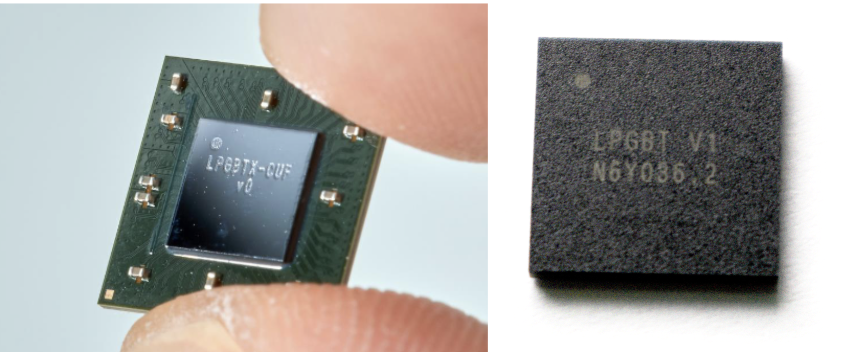
Figure 1: The lpGBT silicon die on the package substrate (left) and the finished product with overmold (right)
The Low Power Giga Bit Transceiver (lpGBT) is a reliable, radiation-tolerant ASIC designed for use in multiple detector systems of the Large Hadron Collider (LHC) (see Figure 1). It will be extensively used in the ATLAS, CMS, and LHCb detectors as well as the accelerator sector to establish versatile and high-speed bidirectional optical links. Depending on the selected operation mode, the ASIC supports a 2.56 Gb/s link from the counting room to the detectors and either a 5.12 or 10.24 Gb/s link from the detectors to the counting room. The lpGBT-link provides a unified physical channel for transmission of Timing, Trigger and Control (TTC); Data Acquisition (DAQ); and Slow Control (SC) information. Its innovative architecture enables the establishment of reliable point-to-point bidirectional optical links with fixed and deterministic latency, ensuring exceptional performance in the challenging radiation environments encountered in high-energy physics experiments at the LHC. Figure 2 depicts the generic architecture of an HEP link that uses the lpGBT. Its main feature is the clear distinction between the on-detector and off-detector system requirements with the on-detector systems having to sustain radiation while the off-detector little or no radiation. This has allowed the freedom for the extensive use of Commercial Of-The-Shelf (COTS) components in the off-detector systems while for the on-detector systems custom devices had to be designed and/or qualified for radiation hardness.
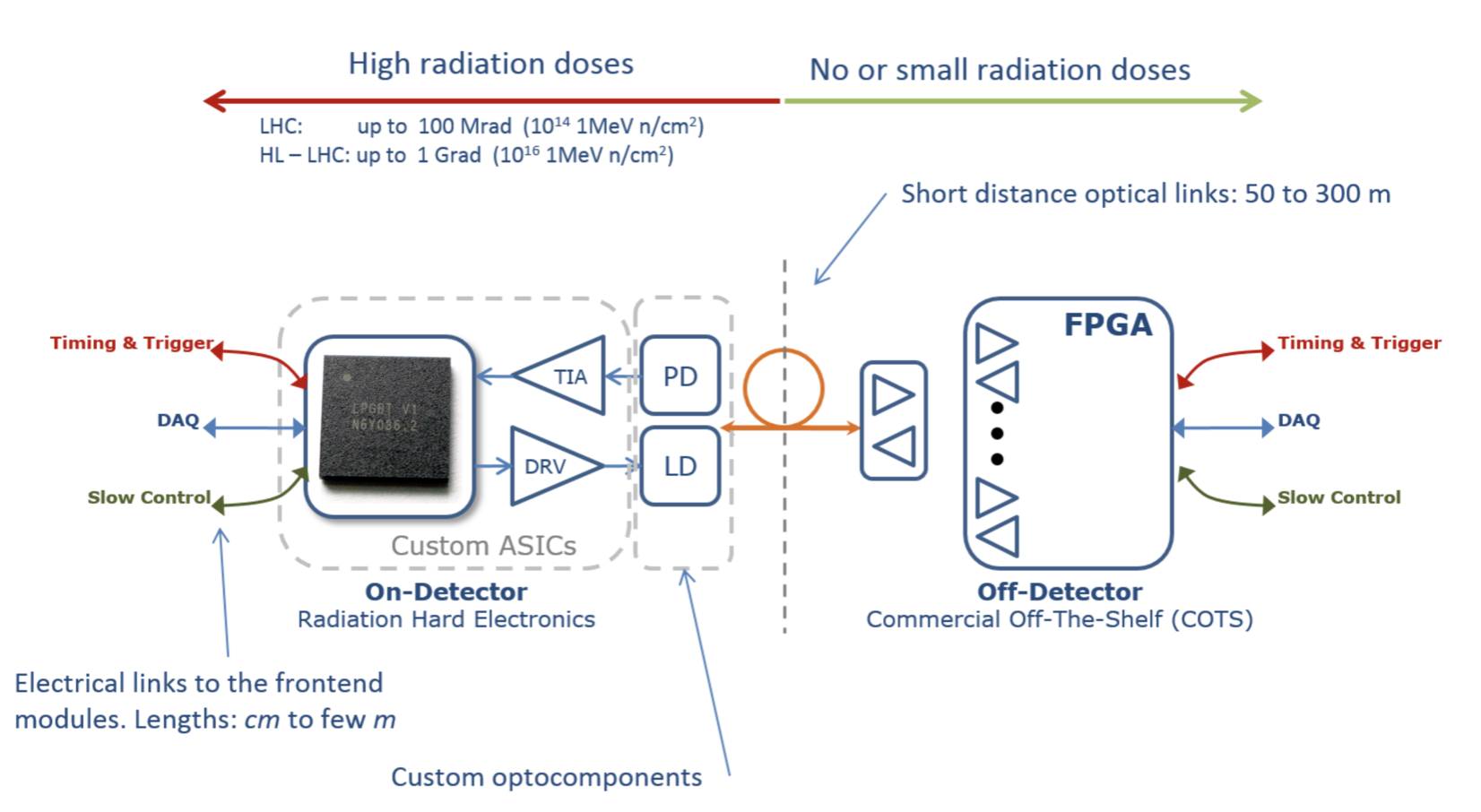
Figure 2. High level block diagram of a radiation-hard optical link incorporating the lpGBT and opto-electronic components.
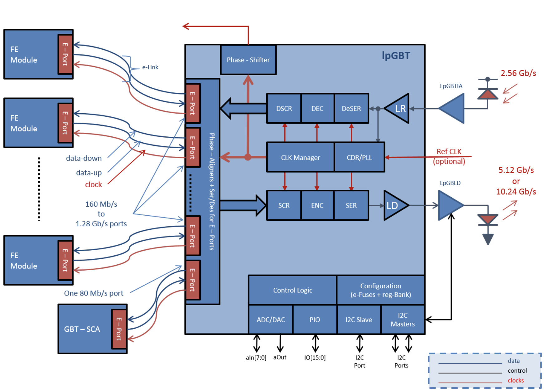
Figure 3. lpGBT ASIC internal block diagram.
Figure 3 provides a block diagram of the internal architecture of the lpGBT, including its main external connections. In its standard setup, the lpGBT collects data from up to 28 ASICs located in the detector area using electrical connections called e-links. This aggregated data is then transmitted through a laser driver ASIC to the off-detector systems. The lpGBT offers a high degree of flexibility, featuring 336 programmable registers, 11 configuration pins, and support for various data rates to meet diverse user requirements. Moreover, the lpGBT incorporates analog peripherals such as digital-to-analog converters, temperature monitoring, programmable I/Os, and I2C drivers to facilitate experiment control and monitoring systems. To ensure reliability in harsh radiation environments, the lpGBT employs triple modular redundancy on the clock tree, reset, combinatorial and sequential logic, safeguarding against single-event effects (logic errors induced by the transit of a single ionising particle present in the radiation environment in a sensitive region of the circuit).
Production
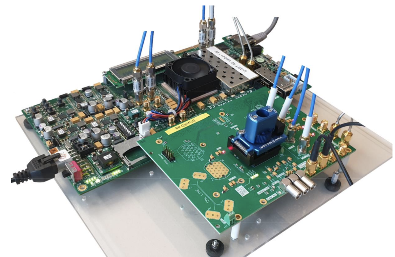
After successfully qualifying the initial prototypes through laboratory and radiation campaigns, a total of 200,000 lpGBT chips were produced. These chips underwent thorough testing at a subcontractor's facility from Q4 2022 to Q1 2023 using an automated IC tester. Figure 4 (left) depicts the IC tester and the computer running the test software. Figure 4 (right) displays the test-board securely attached to the IC tester, providing a socket that receives the devices under test. Once the testing process concludes, the software directs the machine to place each chip on the corresponding tray, labeled as either PASS or FAIL. The excellent yield obtained, 98%, is a testimony of not only the excellent CMOS and packaging technologies used but also of the painstaking design effort, design verification and experimental qualification done during the project development.
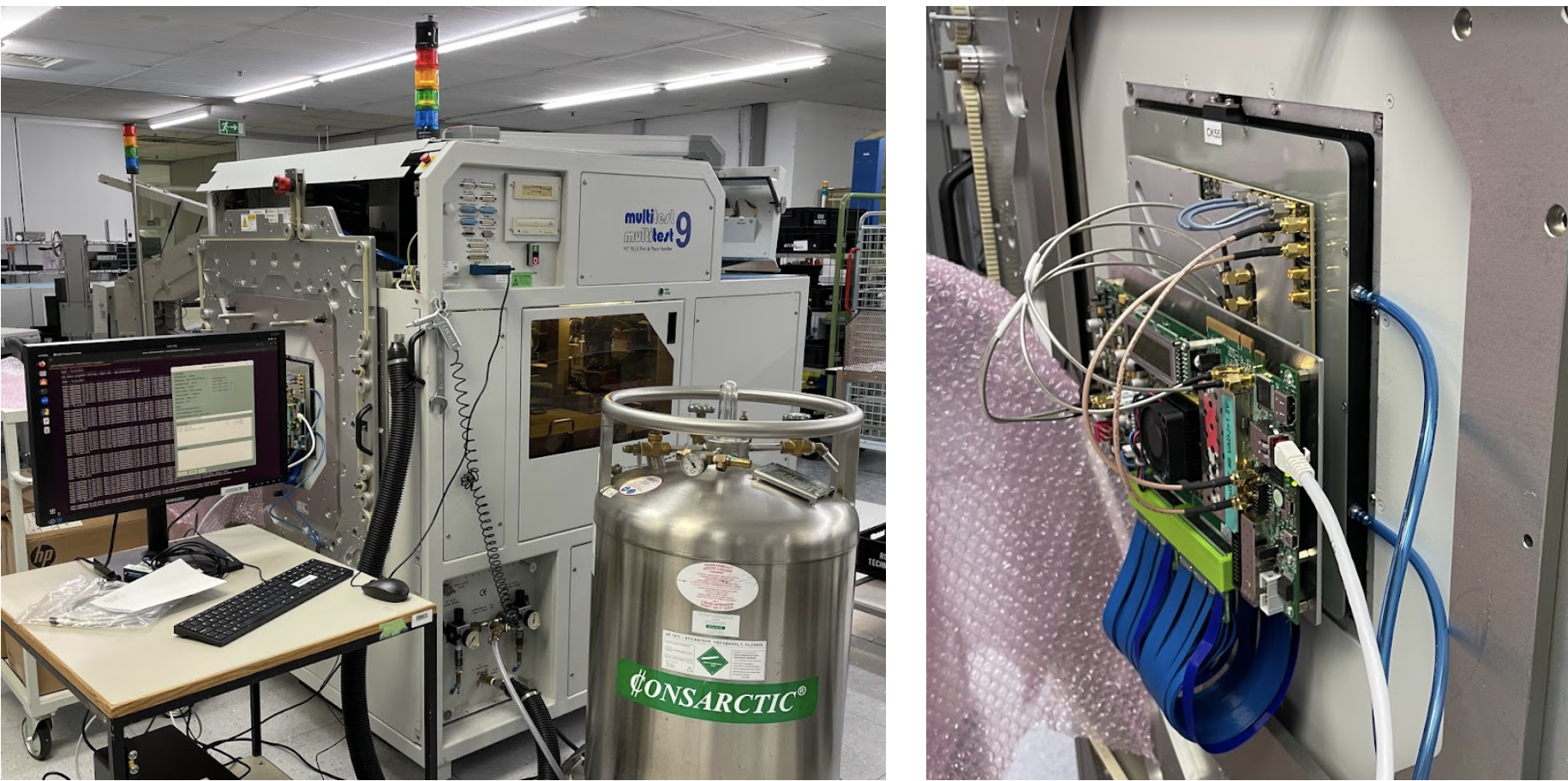
Figure 4 IC tester and the computer running the test software (left) and the test-board mounted on the IC tester (right).
To ensure the delivery of defect-free lpGBT ASICs to end users, a rigorous production testing process was employed. Each chip underwent comprehensive testing using a tailored test suite with a duration of 30 seconds (a compromise between overall test cost and test coverage). The suite encompassed the I/O connectivity and functionality, including triplication. The tests were conducted at three different supply voltages and two temperatures: ambient and cold (-30 °C). Analogue calibration data was acquired at both temperatures, and the resulting data will be made available to the lpGBT users. At the beginning of each test, a unique chip identifier was internally fused (engraved), enabling easy identification of each lpGBT once installed in the detector through slow control mechanisms. The production devices are now being distributed to the experiments who will use them to implement all the optical links in the detectors being upgraded for the HL-LHC programme.
In conclusion, the lpGBT ASIC represents a remarkable leap forward in high-energy physics experiments technology, addressing a demanding need of the LHC's detector systems for error free communication under irradiation. Its ability to establish high-speed bidirectional optical links, robust internal architecture, and exceptional radiation tolerance make it an indispensable asset for scientific research at the LHC. For more details visit https://lpgbt.web.cern.ch).