![]()
The PH electronics support group
The PH-ESE group (Electronics Systems for Experiments) was established in 2007 from the merging of 5 separate PH electronics groups. The group consisting of ~50 staff members supports all CERN experiments with electronics R&D, services and the commissioning and running of their large complex electronics systems. The merging of the PH electronics expertise into one large group has assured sufficient critical mass to keep up with the fast evolving electronics technologies. It has enabled efficient common services to be established and the development of common solutions for our challenging HEP systems and environments (radiation, magnetic field, low mass, etc.). The electronics expertise in the group covers very widely all electronics disciplines from the development of ASICs for specific detectors to the design and maintenance of global power distribution systems needed in large experiments.
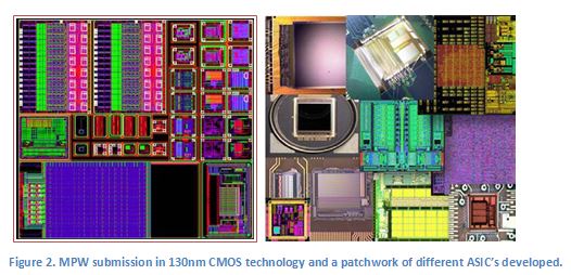
Modern IC technologies, critical to all new HEP experiments, are handled by our IC experts in the ME (Micro-Electronics) section. This spans from designing dedicated front-end ASIC’s for particular detectors (pixels, strips, GEM, etc.), the development and support of ASIC’s developed for the general use in a large multitude of experiments (Link interface chips, power conversion, slow control and monitoring, etc.) to the servicing of the HEP community with appropriate ICtechnologies that can function correctly in our very harsh radiation environments. The critical access to appropriate modern and affordable radiation tolerant IC technologies is assured via a continuous R&D activity and service effort where new IC technologies are evaluated and qualified for radiation hardness and then made available to the world wide HEP community via a MPW
(Multiple Project Wafer) service with associated libraries and design tools. Assuring the necessary training of IC designers and students in our community is also an integral part of this with regular training and workshop events. The use of such common radiation hard technology platforms has been very successfully used by our community for the current LHC experiments (250nm CMOS) and is now being used extensively for the development of ASIC’s for new experiments and phase1 upgrades of the LHC experiments (130nm).
For longer-term developments (e.g. LHC Phase 2 upgrades) the process of qualifying an appropriate new technology (65nm) has started and the accompanying MPW service, libraries and tools will be made fully available over the coming year.
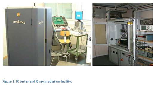
The ME section uses modern CAE IC design tools and have the required facilities for testing and qualifying integrated circuits (IC tester, X-ray irradiation, Wafer probing, etc.).
The FE (Front-End) section covers the critical integration aspects of making on-detector electronics modules and hybrids and integrating them into the experiments. Such modules must for HEP be extremely compact, low mass and highly reliable which requires special PCB/hybrid technologies to be used together with the critical interconnections between the detector itself and the front-end ASIC’s that are often used as bare die IC’s. The section also has the required expertise for front-end system integration aspects covering low mass power distribution and electromagnetic interference/compatibility (EMI/EMC). The front-end section has a wide set of electronics instrumentation and electronics labs to develop, test and debug front-end electronics systems.
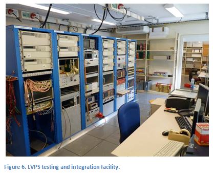
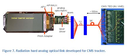
The BE (back-end) section covers the domain of off-detector electronics systems and the optical links required to transport large data quantities, typical of modern HEP, to the DAQ and trigger systems. This includes expertise related to opto-electronics components (laser, optical receivers, fibers) and their behavior in our harsh radiation environments. Our link activities cover the support of optical links in several experiments and the support of the current TTC systems, extensively used in all LHC experiments. A new radiation hard high speed optical link is under development in close team work with our ASIC designers. Expertise and activities related to the design of crate based DAQ interface and trigger processing systems made from large electronics modules based on modern FPGA’s are also concentrated in this section. General electronics infrastructure required for large experiments covering electronics racks and crates (e.g. VME and TCA) and radiation tolerant power supply systems are supported. Finally the very popular electronics pool rental service enables all CERN users to get quick and easy access to a very large set of electronic modules and instrumentation covering from high end oscilloscopes, over modular instrumentation to crates and power supplies.
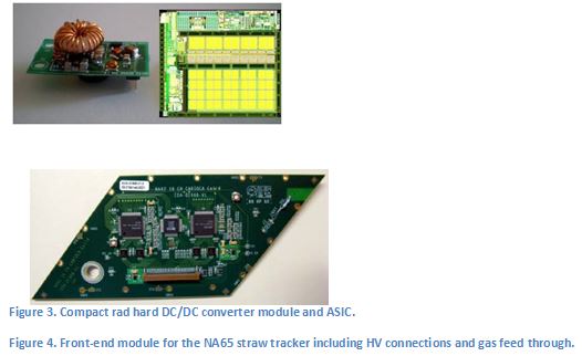
Approximately half of our manpower resources are used to supply electronic services and support (pool, LVPS, IC technologies) and develop and support common/generic ASIC’s and sub-systems across a large set of different experiments ( TTC, ELMB, Radiation hard link, power supplies, power distribution and on detector power conversion). The remaining half of the group resources are allocated to develop, commission and run dedicated electronics ASIC’s/systems for particular experiments and sub–detectors (ATLAS tracker, ATLAS trigger, CMS tracker, CMS preshower, CMS 6
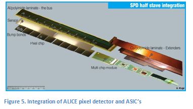
muon, ALICE pixel, ALICE TPC, ALICE readout link, LHCb RICH, LHCb Vertex , NA62 GTK, straws and calorimeter, plus more) in close collaboration with the experiment groups in PH, external institutes and with the help of students and fellows. The group is also involved in the development of novel hybrid and monolithic pixel detectors of which some are used by industrial partners as part of the CERN technology transfer program.
As part of our integration into a single electronics support group we have recently finalized our relocation of the whole group and related infrastructure into a central area in building 13/14 where we are in the process of finalizing the required refurbishment of the buildings and infrastructure. When this refurbishment is fully finalized (~6 months more to go) we will be pleased to invite you to an open-house day for you to get a chance to know us better and see our “new electronics headquarter” with its labs and offices.
We will also be very pleased to see you in our regular PH-ESE electronics seminars on Tuesday mornings and then join us for a coffee in our small local coffee corner in building 13. You are very welcome to register on our PH-ESE seminar mailing list to be informed about coming seminars and we will also be very pleased to receive your proposals for possible future seminars in the electronics domain. For more information on the group and our projects you can finally take a look on our group website.