Probing Noise Sensitivity in FBCM: From ASIC Design to EMC Testing Teaser:

Sketch of the FBCM location behind the last disk of the inner tracker (left) and a zoom to the two FBCM half discs forming a ring around the beam pipe with a detailed representation of the components on each service quadrant (right).
The accuracy of the luminosity measurement is an important challenge in modern accelerator science. The luminosity describes how “bright” the beam is; in other words, how many particles travel in the beam. The higher luminosity increases the interaction rate per collision [1]. From the physicist's point of view, the luminosity measurement is critical, as it directly impacts the accuracy of the physics analysis. In the upgraded CMS experiment, the uncertainty of the luminosity measurements is required to be below 1% [2]. Hence, data from multiple parallel systems will provide the required measurement accuracy. One of those systems is Fast Beam Condition Monitoring (FBCM).
The FBCM system is a trigger-independent, bunch-by-bunch luminosity and beam-induced background (BIB) meter system. It will provide 1 ns (RMS) time resolution for sub-bunch measurement and beam halo separation. The system is divided into four half-disks, forming two disks at both CMS detector sides (one on +Z and one on −Z), mounted to the last outer tracker disk. Each FBCM disk has four service boards with an IT-portcard (including LpGBT chips [3] , used for reading out hybrid modules) and a DC-DC converter. The service board is connected to three hybrids, hosting two dedicated FBCM23 ASICs connected to six 1.7×1.7 mm2 silicon diodes. Detectors will form two rings with a 14.5 cm radius, from which the luminosity will be extrapolated [4][5]. Because of the proximity of the beam, the Front-End electronics must provide good radiation hardness because of the total irradiating dose of up to 200 MRad and fluence 2.5 × 10¹⁵ Neq.
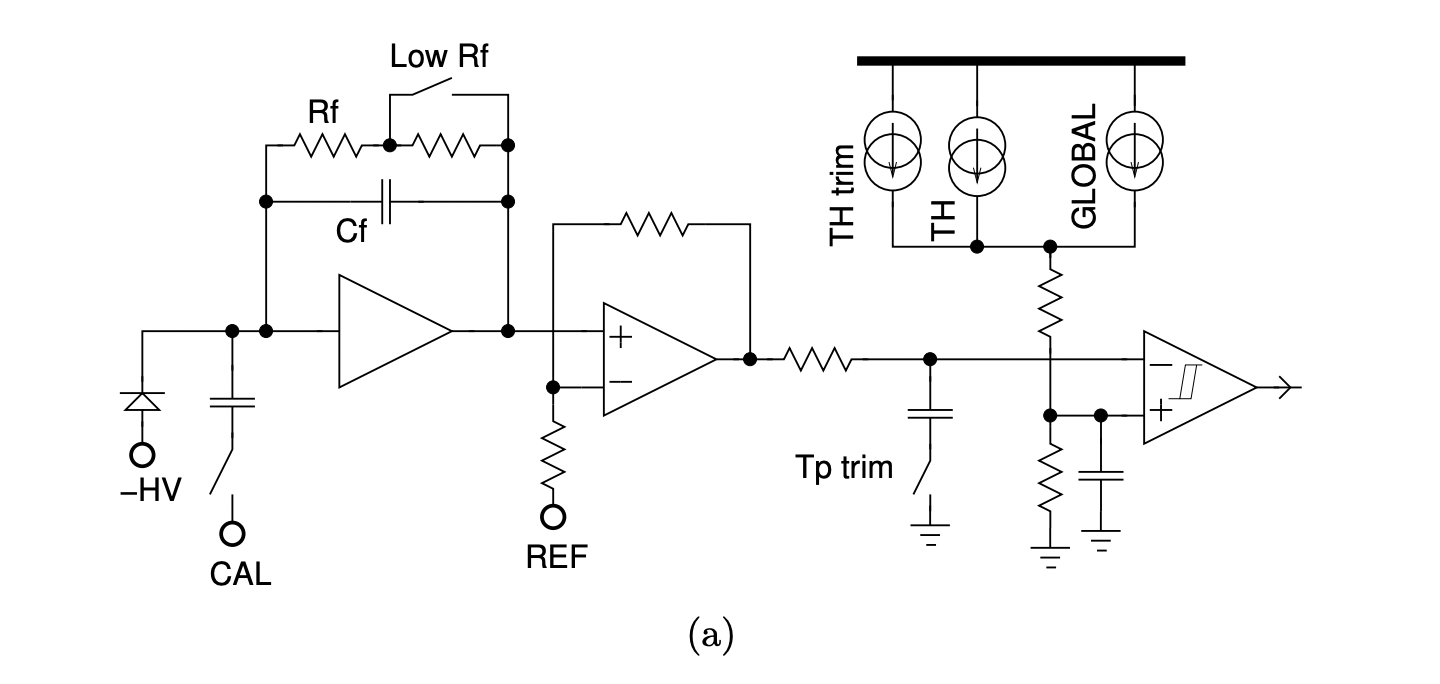
The FBCM23 design started in April 2022 and the ASIC was successfully sent to production in May 2023. The chip implements six analog channels, each consisting of a two-stage amplifier, RC filter, and comparator. The signal processing chain is shown in Fig1a. The working principle is as follows: the charge-sensitive amplifier (CSA) reads the charge generated in the detector by the impinging particle and then amplifies and shapes it (shaping improves the signal-to-noise ratio). Then, the second stage (booster) provides an additional gain to the system. Finally, a programmable RC filter allows for a tradeoff between speed and noise. At the end of the channel, the signal is compared with the user-controlled threshold, and the binary output is sent via SLVS interfaces off the chip. This type of front-end electronics is called “binary,” as it provides only information if the signal is higher or lower than the threshold. Because of the simple yes/no information available at the output of the chip, another circuit must be incorporated to extract the timing information from the provided signal. The system uses an lpGBT ASIC[3] to sample FBCM23 ASIC output and extract time-of-arrival and time-over-threshold (ToA, ToT) numbers.

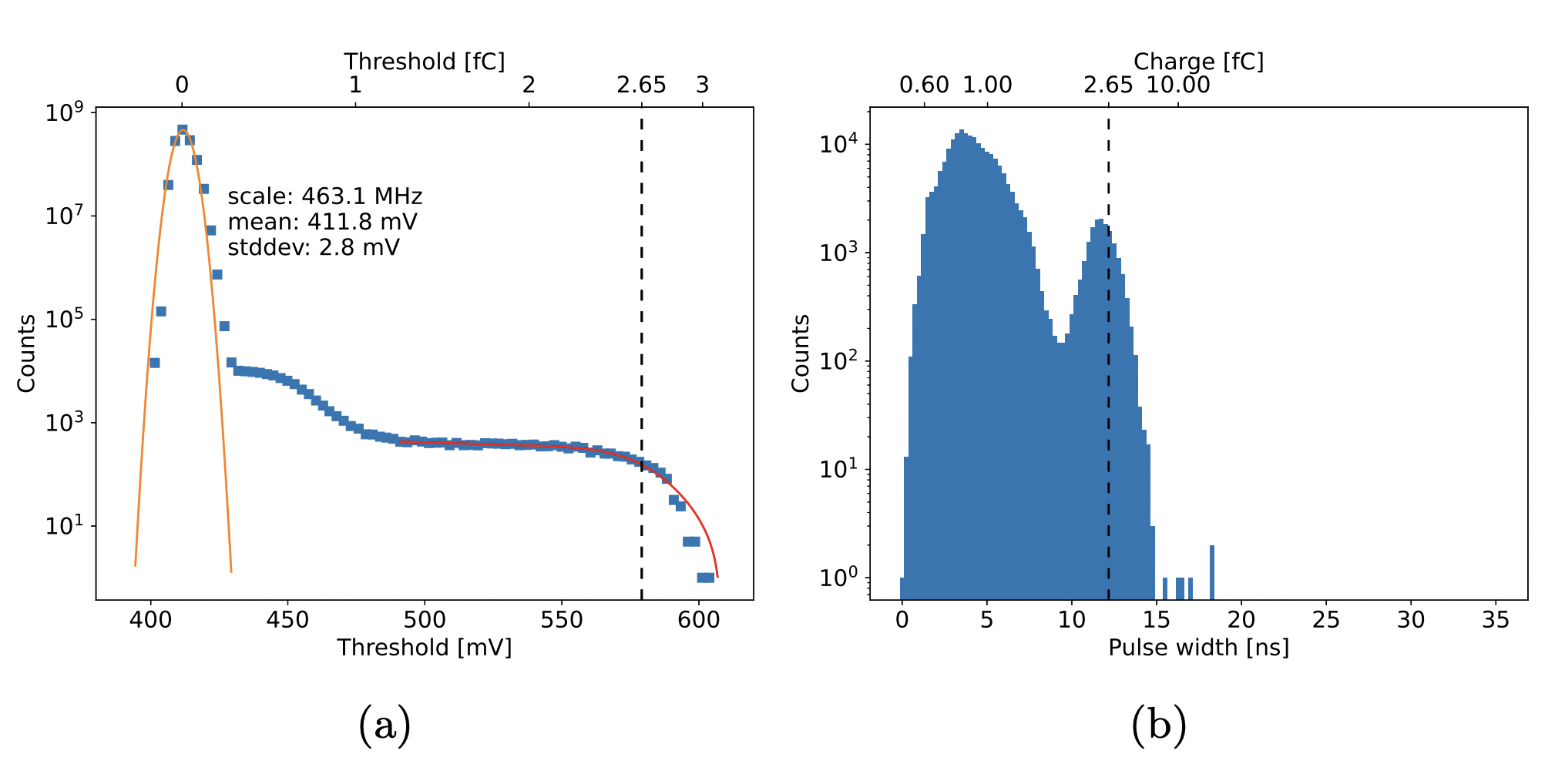
The designed chip was delivered from the efoundry in June 2023. Evaluating basic parameters, like DAC characterization, gain, and noise extractions, shows excellent performance and follows simulation data. We want to emphasize the ASIC noise performance; thanks to careful design using the EKV model [6] and noise analysis, we achieved a noise level of 550 electrons where 800 electrons were required. In Figure 2a, you can see an example of a threshold scan with a radioactive source (Americium-241), visible baseline noise (high peak), and two slopes from the signal: the first one that corresponds to lower energy peaks and the second that corresponds to the 60 keV line. In the following Figure 2b, one may see the ToT (pulse width at the ASIC output) histogram for one particular threshold setting. The dotted line should match with the histogram peak. The difference is about 5%, which corresponds to the detector charge collection efficiency (later proved by the BRIL group and TCT measurements). This type of test is sometimes called absolute calibration, as we use a radioactive source with well-defined gamma photon energies.

Figure 2: Threshold scan using radioactive source 241Am
After a successful characterization process, the time has come to test the ASIC in a semi-final system on the test beam. The BRIL group (CMS) prepared the required telescope, DAQ, and all other hardware and software and performed the test. The first insight into data shows excessive pick-up noise in the ASIC. The test team could not work with threshold settings below two femto-Coulombs (where a 0.7 fC threshold is required). We agreed that the detector module is sensitive to external disturbances and that we need to find a solution to lower its impact on the analogue performance.
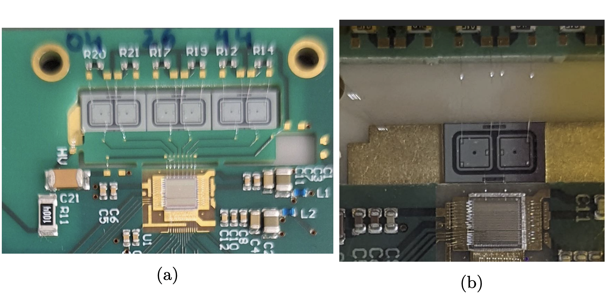
Thanks to Daniel Valuch (SY-RF-BR) and his readiness to help and his great experience, we had an opportunity to use his SY-RF’s EMC lab, which contains all necessary equipment, including RF generators, amplifiers, power meters, the anechoic chamber, antennas, and EM clamps. As a preparation for the test, we did additional ASIC sensitivity simulations. Based on the results, we predicted two possible scenarios: first, the external disturbances are passing to the ASIC through the power lines, and second, when they pass to the chip input and then are amplified (because of the high-speed amplifier, peaking time in the order of 6 ns). To test these hypotheses, we prepared four different samples:
- Reference sample, not connected to the sensor, additional screen on backside
- Sample with sensor connected through the fanout + screen on backside
- Sample with direct bonding between sensor and ASIC + screen on backside
- Same as sample 2 but without backside screen (configuration used in beam test)

Figure 3: Samples used in the EMC test (a) sample 2 and (b) sample 3.
For the disturbances coming through the power lines, we may expect to see pick-up noise in all four samples for frequencies ranging from 5-100 MHz. While for the second option, we expect to see a pick-up in the 20-100MHz range. The lab test bench allows working with a conducted noise (injected using an electro magnetic (EM) clamp to the power cables) up to 20 MHz and radiated noise (emitted using an antenna) from 50 MHz and above.

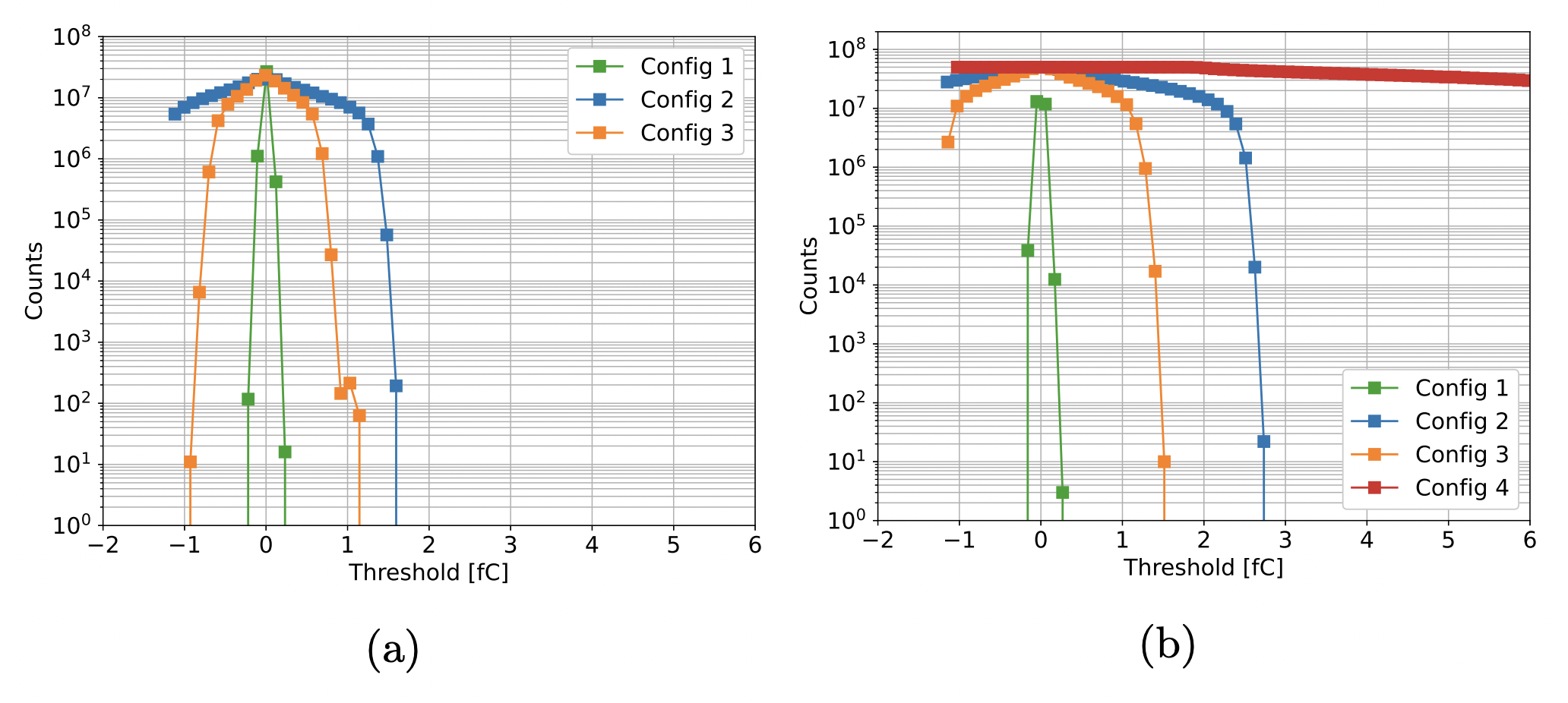
Figure 4: EMC tests results for (a) conducted and (b) radiated noise.
The results for both measurements are shown in Figure 4. Here come two main observations: first, the control sample (config 1) is all the time clean, what means that disturbances is not passing through the power lines. Second, the direct bonding shows better performance than pitch-adaptor option, what means that the pick-up noise depends on the sensor-to ASIC input connection length.
Additionally, in Figure 4b, one may see that the pick-up noise for the sample used during the beam test (config 4) is even higher than for the same sample with an additional screen on the backside. In the case of screen absence, the cooling pipe is floating and acts as a big antenna, increasing sensitivity to external electromagnetic interferences.
Summarizing the measurements, one can conclude that the conducted and radiated noise is propagating through the front-end inputs and ground reference. The reference sample with the floating inputs is insensitive to the radiated and conducted noise up to the levels used in the measurements: fields up to 10 V/V and common mode currents up to 50 mA. The best-case configuration module (direct bonding to the sensor) can tolerate up to 5 mA common mode currents with a minimum operating threshold of 1 fC and field strength up to 1 V/V (120 dBµV/m) with a minimum operating threshold of 0.7 fC. These numbers have to be compared to the CISPR 22 standard for the common mode currents for industrial equipment emissions, which are 100 µA (above 500 kHz), and the CISPR A industrial environment limits for emission at 1 m distance, which is 55 dBµV/m.
In summary, the FBCM23 ASIC demonstrated excellent performance in initial characterization. The study found that direct bonding between the sensor and ASIC, along with proper shielding, significantly improves noise resilience. The optimized configuration performs robustly even under conditions exceeding industrial EMC standards, confirming its suitability for deployment in the CMS environment. These findings will inform further optimization to ensure the reliable operation of the FBCM system under CMS experimental conditions.
References
[1] K. M. Potter, “Luminosity measurements and calculations; 1994 ed.,” 1994.
[2] CMS Collaboration, “The Phase-2 Upgrade of the CMS Beam Radiation Instrumentation and Luminosity Detectors,” tech. rep., CERN, Geneva, 2021. This is the final version, approved by the LHCC.
[3] S. Biereigel, S. Kulis, R. Francisco, P. V. Leitao, P. Leroux, P. Moreira, and J. Prinzie, “The lpGBT PLL and CDR Architecture, Performance and SEE Robustness,” PoS, vol. TWEPP2019, p. 034, 2020.
[4] M. Sedghi and on behalf of the CMS Collaboration, “Fast beam condition monitor of the CMS experiment at HL-LHC,” Journal of Physics: Conference Series, vol. 2374, p. 012011, nov 2022.
[5] G. Auzinger, H. Bakhshiansohi, A. Dabrowski, A. Delannoy, A. Dierlamm, M. Dragicevic, A. Gholami, G. Gomez, M. Guthoff, M. Haranko, A. Homna, M. Jenihhin, J. Kaplon, O. Karacheban, B. Korcsmáros, W. Liu, A. Lokhovitskiy, R. Loos, S. Mallows, J. Michel, V. Myronenko, G. Pásztor, M. Pari, J. Schwandt, M. Sedghi, A. Shevelev, K. Shibin, G. Steinbrueck, D. Stickland, B. Ujvari, and G. Wegrzyn, “The cms fast beam condition monitor for hl-lhc,” Journal of Instrumentation, vol. 19, p. C03048, mar 2024.
[6] C. C. Enz and E. A. Vittoz, Charge-based MOS transistor modeling: the EKV model for low-power and RF IC design. John Wiley & Sons, 2006
