![]()
Silicon-detector modules for future experiments
The strategic EP R&D programme on technologies for future experiments pursues an ambitious development programme for advanced silicon detectors. Achieving reliable, high-performance, large-area tracking and timing detector systems with minimal material content and affordable cost presents major challenges. These challenges include hybridizing sensors and readout ASICs, as well as integrating detectors into functional modules, both of which are addressed in Work Package 1.3 (Modules).
Building upon ongoing efforts within the EP department, the activities in Work Package 1.3 encompass a comprehensive exploration of enabling technologies, critical for their success. This includes:
- the investigation of advanced and scalable interconnection techniques on chip and module level,
- post-processing methods and packaging solutions and
- the building of demonstrator assemblies and modules.
Central to the project’s objectives are rigorous testing and qualification procedures of these demonstrators, including novel and state-of-the-art inspection and metrology methods.
WP1.3 comprises a team of approximately 10 students, fellows, and CERN staff that contribute part-time to this activity. A key factor is the various contributions from institutes and industrial partners collaborating among others within the European AIDAinnova project. WP 1.3 also fosters strong links to the other silicon Work Packages of the EP R&D programme. The diverse team collaborates on research, design, testing, and implementation of silicon modules for various applications, targeting future upgrades of particle physics experiments conducted at CERN’s Large Hadron Collider (LHC) and proposed future accelerator facilities such as CLIC and FCC.
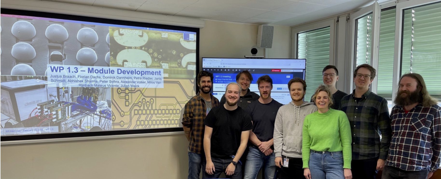
Figure 1: The WP 1.3 students and fellows in early 2023.
Activities
During phase 1 of the EP R&D programme from 2020 to 2023, the WP 1.3 activities have focused on advancing the tools and methods for innovative interconnect and module-integration concepts, resulting in several proof-of-concept achievements [1]. Highlights of these activities are discussed below, along with the extensive testing and characterisation campaigns that validated the feasibility of the developed concepts.
Plating Studies
To ensure reliable connections, electrodes and metal pads must be preprocessed for different interconnection methods. One promising approach involves Electroless Nickel Immersion Gold (ENIG) plating, an in-house process that achieves consistent plating on aluminum electrodes across various applications.
Producing the desired plating height and uniformity was first tested in a large-scale PCB production line and then moved to a better-controlled lab environment with plating solutions specific to the targeted silicon devices [2].
The current setup located in the EP-DT Micro-Pattern Technologies lab is shown in Fig. 2 and can be used for different prototype chips and sensors without the need to process full-size wafers. This opens the possibility for fast interconnection prototyping at the assembly and module levels using different methods, as described in the next sections.
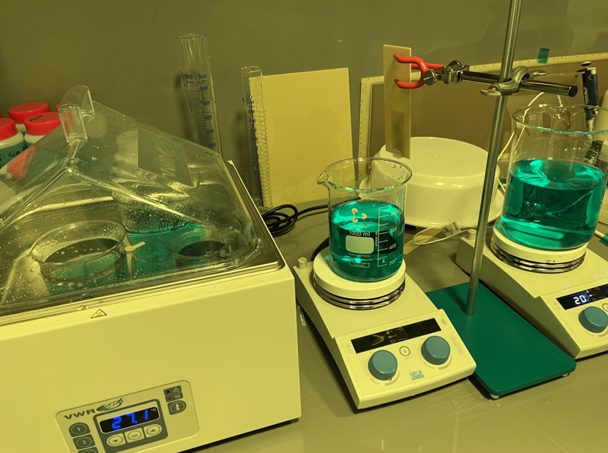
Figure 2: Setup for electro-less nickel deposition in the EP-DT Micro-Pattern Technologies lab, with water bath on the left and two hot plates with forced convection on the right.
For optimal plating quality, WP1.3 has also used advanced microscopic techniques like Energy-Dispersive X-ray Spectroscopy (EDS) (see Fig. 3) to analyze the plating process meticulously. This systematic approach has led to consistent plating results, even for interconnection pitches as fine as 50 microns, achieving the desired uniform plating height across various applications.
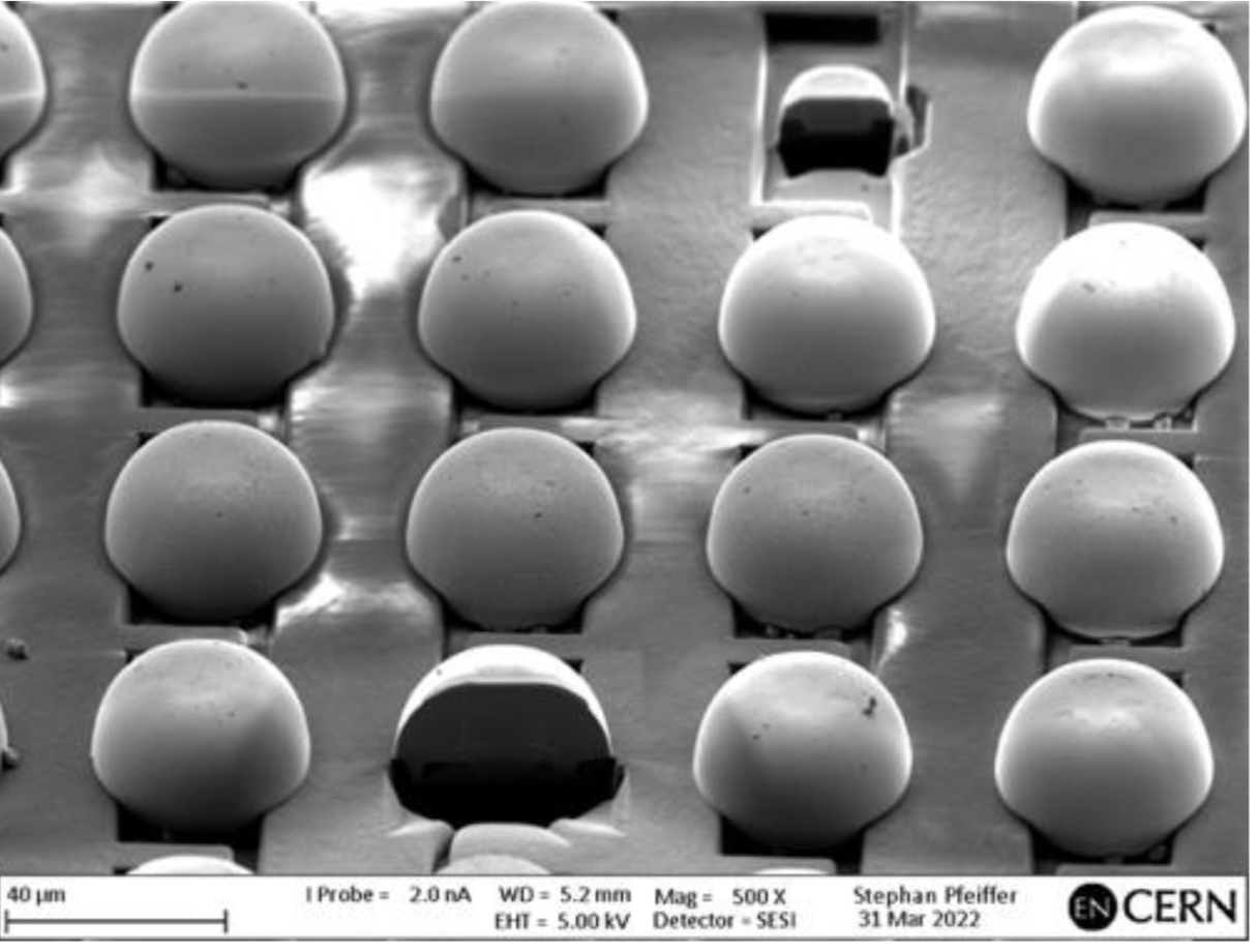
Figure 3: Investigation of ENIG plating on a Timepix3 ASIC, using Energy- Dispersive X-ray Spectroscopy (FIB-SEM EDS).
Fine-pitch hybridisation with tin/silver bump bonding
Bump-bonding is an industry standard used to achieve high-density connection of pixels in semiconductor detectors. This technology requires the processing of full wafers for both under-bump metal and solder deposition, making it unusable for individual devices. For this reason, a replacement process targeting single-die bonding has been investigated together with Fraunhofer IZM.
The SnAg support-wafer solder bump-bonding process developed at IZM has been tested using single dies of CLICpix2 ASICs (containing 128x128 pixels with 25 microns pixel pitch) and active-edge sensors produced at FBK. Successful bonding has been performed for a range of sensor thicknesses from 50-130 microns. Non-destructive inspection and failure analysis has been performed using an X-ray system (Fig. 4), and the device performance has been evaluated both in laboratory and particle-beam tests. Fully-efficient detection of minimum ionising particles and interconnect yields above 99.7% have been achieved for all tested assemblies [3].
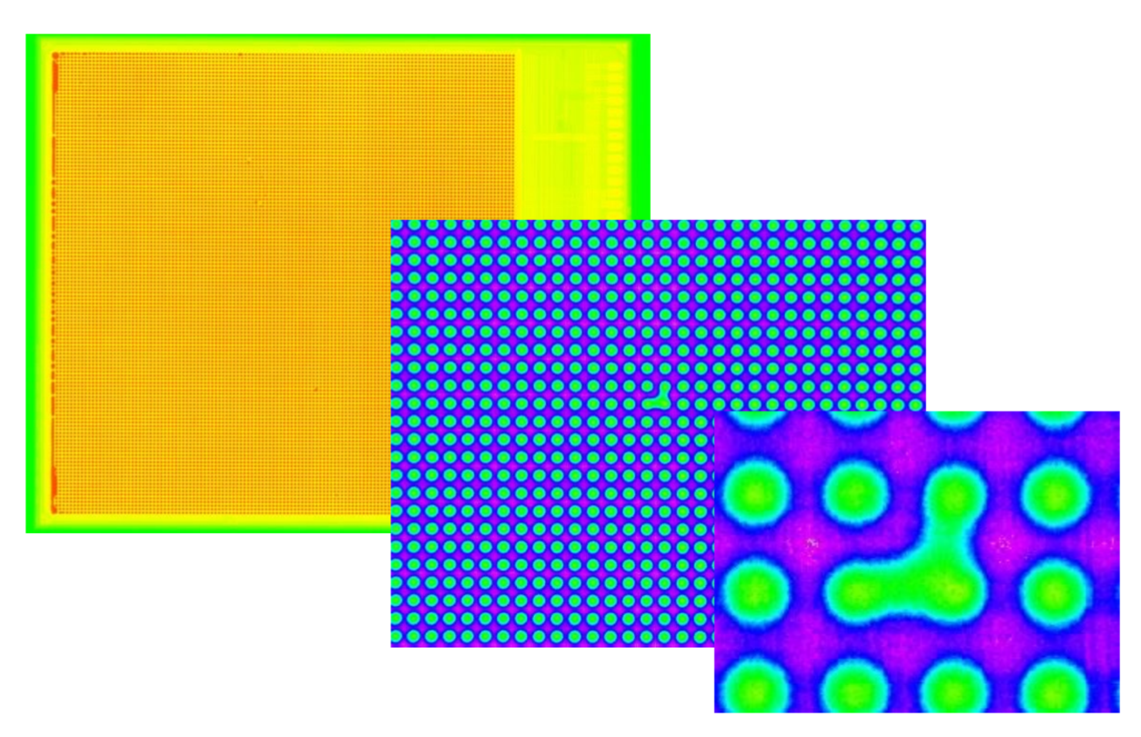
Figure 4: X-ray image of the bump bonds inside a CLICpix2 hybrid pixel- detector assembly with 25 microns pitch and a matrix size of 3.2 mm x 3.2 mm. A cluster of 3 shorted pixels is visible.
Hybridisation and module assembly with adhesives
The use of Anisotropic Conductive Adhesives (ACA) for cost-effective in-house pixel-detector hybridisation is studied as an alternative to standard bump-bonding processes. The ACA technology is adapted from industry, where it is commonly used for LCDs with single rows of connections. Both, film-based (ACF) and paste-based (ACP) adhesives with embedded conductive microparticles are studied. For large-pitch applications with suitable bonding-pad topologies, also epoxy-based Non-Conductive Paste (NCP) is under study.
The in-house fabrication of hybrid assemblies and modules is performed at Geneva University DPNC, using a flip-chip device bonder shared between CERN and Geneva University (Fig. 5). The machine allows for bonding with micrometer precision and using controlled force and temperature profiles, as required by the respective interconnect technique. Fig. 6 shows a cross-section through a hybrid assembly of a Timepix3 readout ASIC with a planar silicon sensor, bonded with ACF. Functional Timepix3 ACF assemblies have been successfully operated in laboratory setups and exposed to particle beams (Fig. 7).
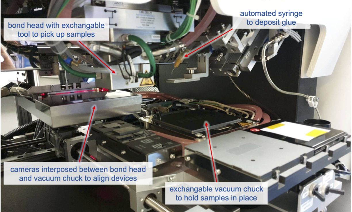
Figure 5: Flip-chip device bonder at the University of Geneva DPNC.
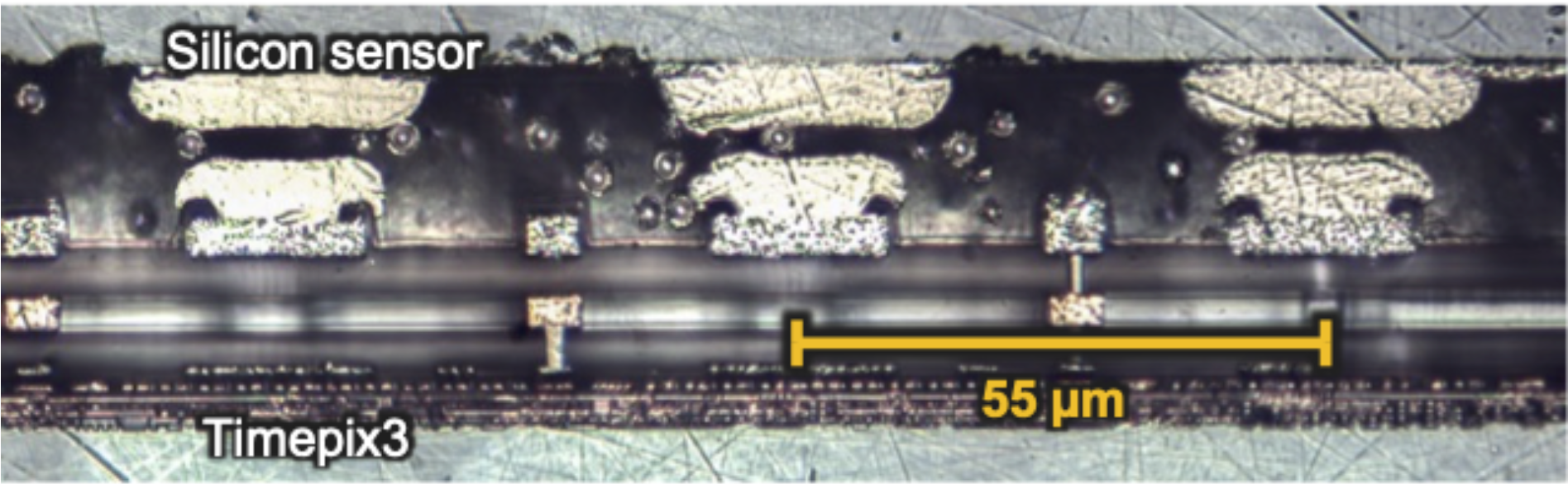
Figure 6: Cross-section of Timepix3 ACF assembly, with conductive micro particles embedded in a thin epoxy film connecting the sensor and readout-ASIC pixels with a pitch of 55 microns.
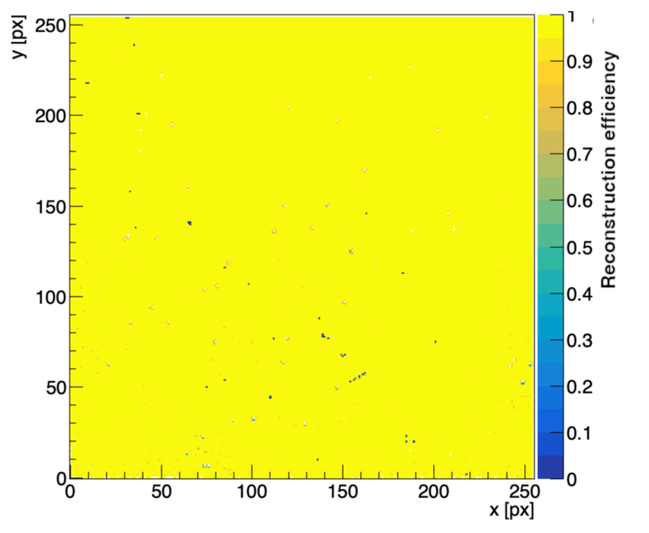
Figure 7: Reconstruction efficiency for high-momentum particle tracks passing through an ACF-bonded Timepix3 assembly. The high efficiency uniformly distributed over the 14 mm x 14 mm large matrix indicates a successful interconnection between sensor and readout ASIC.
Similar proof-of-concept ACF and ACP assemblies have been produced for the SPHIRD project at ESRF at 50 microns pitch and for ALTIROC2/3 ASICs with Low-Gain-Avalanche Detectors (LGAD) at 1.3 mm pitch. The bonding process is further optimised using dedicated daisy-chain devices, which allow for simplified measurement of the interconnect yield and electrical resistance.
Module integration with advanced interconnection techniques
To achieve a dense integration of pixel chips inside modules, it is essential to minimize the inactive distance between the dies on a module. A flip-chip approach to build modules has been investigated as an alternative to standard module mounting techniques based on wire bonding, aiming to build highly compact modules with minimum inactive area and with a scalable process to achieve large area modules.
Three interconnection techniques based on either ACF with Ni/Au pad plating or NCP with gold-studs on aluminum pads (Fig. 8) or copper-based nano wires on aluminum pads (Fig.9) have been studied using MALTA2 chips and test structures. The flip chip assembly has been carried out on the device bonder shown in Fig. 9.
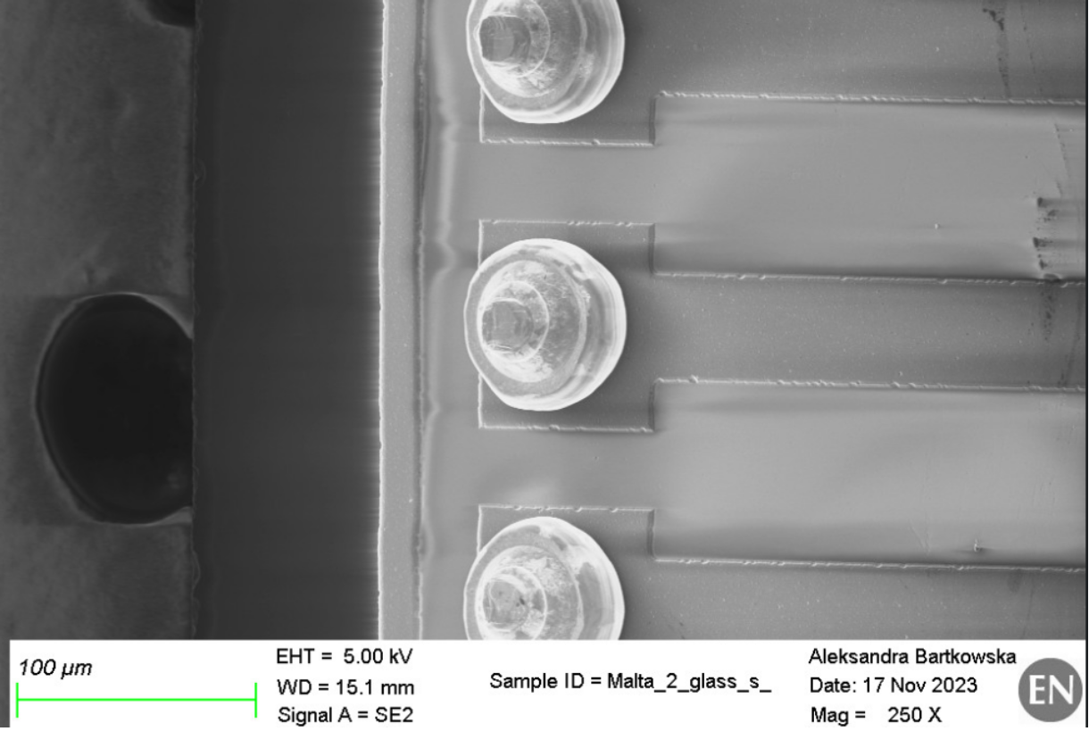
Figure 8: MALTA2 test structure, processed on fused silica at CMi with applied gold studs visible on the three bonding pads in the middle of the picture.
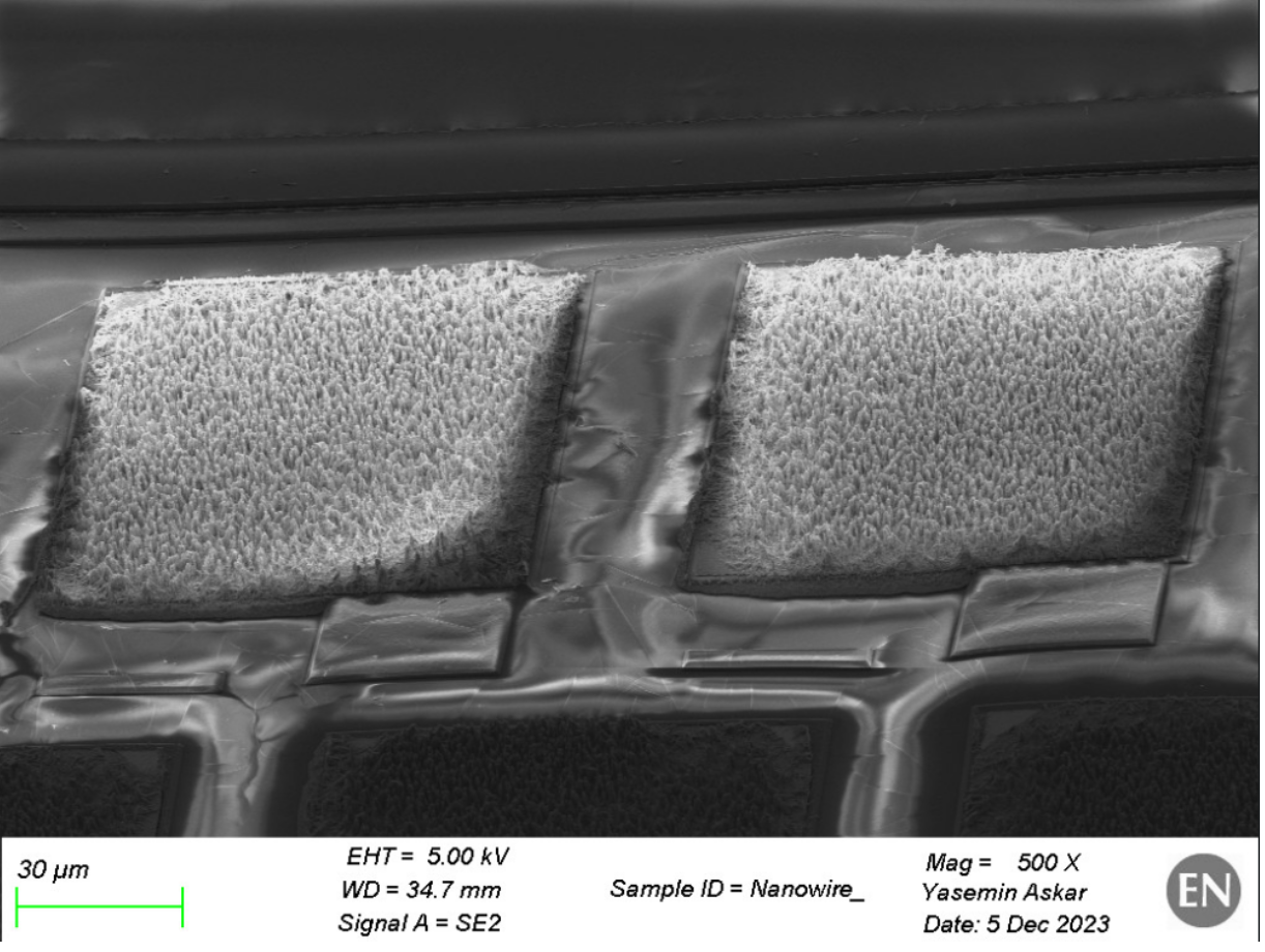
Figure 9: Cu-based nanowires on two MALTA2 pads.
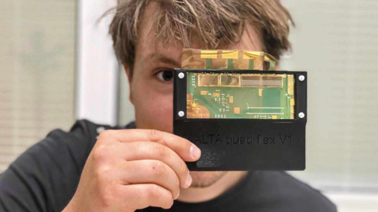
A dedicated flip-chip bondable flex PCB with trace spacings down to 17 microns has been developed [4] which can accomodate up to 4 MALTA2 pixel chips (Fig. 10). Trace routing on the flex is further reduced by using direct chip-to-chip data transfer to the end of the module.
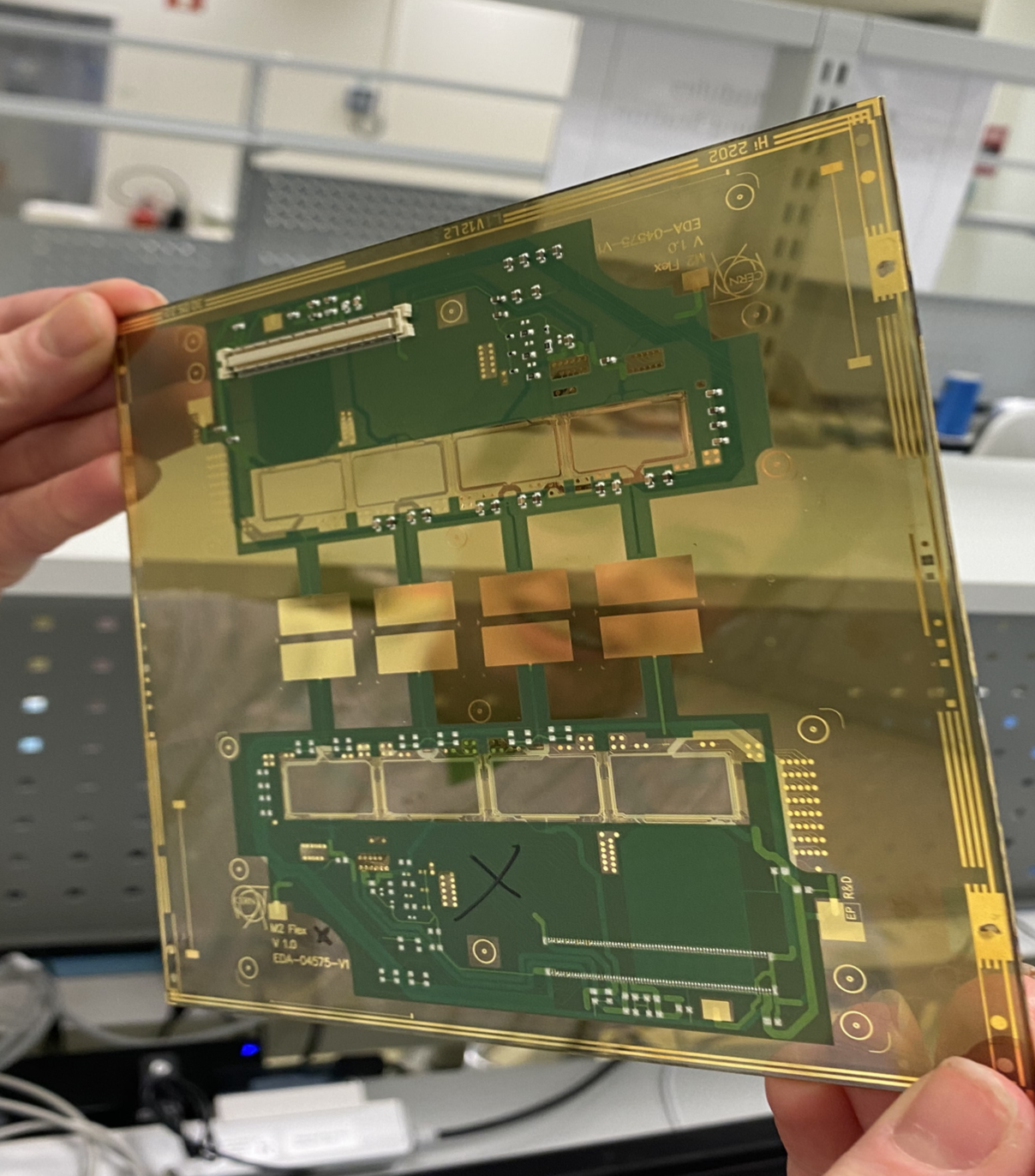
Figure 10: Flex PCB for 4 MALTA2 chips.
The quality and robustness of the flex PCB have been confirmed by bonding a dummy test structure successfully onto the flex using ACF. An electrical evaluation of the test structures has confirmed a high interconnection yield. Functional tests have been performed for MALTA2 sensors bonded onto an assembled flex. Peel-off tests are ongoing, to assess the influence of the bonding process parameters on the mechanical robustness of the module.
Future Plans
Building on the successful proof-of-concept work achieved in the first phase (2020-2023) of the EP R&D programme, Work Package 1.3 has secured an ambitious plan for the second phase (2024-2028) [5]. This next phase prioritizes demonstrating the scalability and reliability of the developed interconnect and module-building methods. Additionally, it explores promising new technologies and upgrades crucial infrastructure, like the flip-chip equipment and multi-module test systems. Strong collaborations with existing detector R&D projects and the newly formed international DRD3 collaboration on silicon-detector R&D will fuel these activities.
References
[1] G. Aglieri et al., Strategic R&D Programme on Technologies for Future Experiments - Annual Report 2023 and Phase-I Closeout, 2024. To appear as CERN-EP-RDET-2024-001
[2] A. Volker et al., Pixel detector hybridization and integration with anisotropic conductive adhesives. To appear in IPRD23 proceedings, 2024. arXiv: 2312.09883
[3] P. Svihra et al., Development of novel single-die hybridisation processes for small-pitch pixel detectors. Journal of Instrumentation 18.03, 2023, p.C03008.1366. doi 10.1088/1748-0221/18/03/C03008
[4] J. Weick et al. Development of novel low-mass module concepts based on MALTA monolithic pixel sensors. JINST 18.04, 2023, p. C04003. doi: 10.1088/1748-0221/18/04/C04003
[5] C. Joram et al., Extension of the R&D Programme on Technologies for Future Experiments., 2023. CERN-EP-RDET-2023-001.