![]()
Silicon Photonics Circuits for Integrated Optical Readout of future High Energy Physics detectors

Fibre optic links are crucial in High Energy Physics (HEP) experiments, allowing the transmission of large volumes of data from particle detectors operating in harsh radiation environments to radiation-free zones.
Silicon Photonics (SiPh) [1] has emerged as a promising optoelectronic technology for next-generation optical readout systems for future CERN detectors. SiPh leverages CMOS foundries to manufacture photonic integrated circuits (PICs) into silicon chips. Compared to the current generation of data links for CERN detectors, which are based on discrete optoelectronic components [2], PICs offer higher radiation tolerance, higher bandwidth, lower power consumption, and lower mass. All these aspects make them particularly attractive for integration in the innermost layers of particle detectors.
The Strategic R&D Programme on Technologies for Future Experiments (EP R&D) [3] of the EP Department includes a work package (WP6) focusing on radiation-tolerant high-speed links. The conceptual target of the project is illustrated in Figure 1, where the PIC is co-packaged with the particle sensor readout circuit (ROC) [5][6][4]. Figure 1 illustrates a wavelength division multiplexing (WDM) scheme, where four optical data signals, each at a different wavelength, are transmitted through a single fibre. The data from the particle sensor is serialised into four channels, each operating at 25.6 Gb/s, and is converted into optical signals using silicon Ring Modulators (RMs) [7]. A commercial off-the-shelf (COTS) WDM receiver is used at the back-end. A key feature of this design is the use of an external laser source (ELS) located in a low-radiation or radiation-free zone. Placing the laser remotely copes with the limited radiation tolerance of lasers and eliminates the electrical power consumption of the light source near the particle sensor. Extensive irradiation testing and device modelling [8][9][10][11] have demonstrated that Silicon Photonics components are tolerant to high levels of radiation.
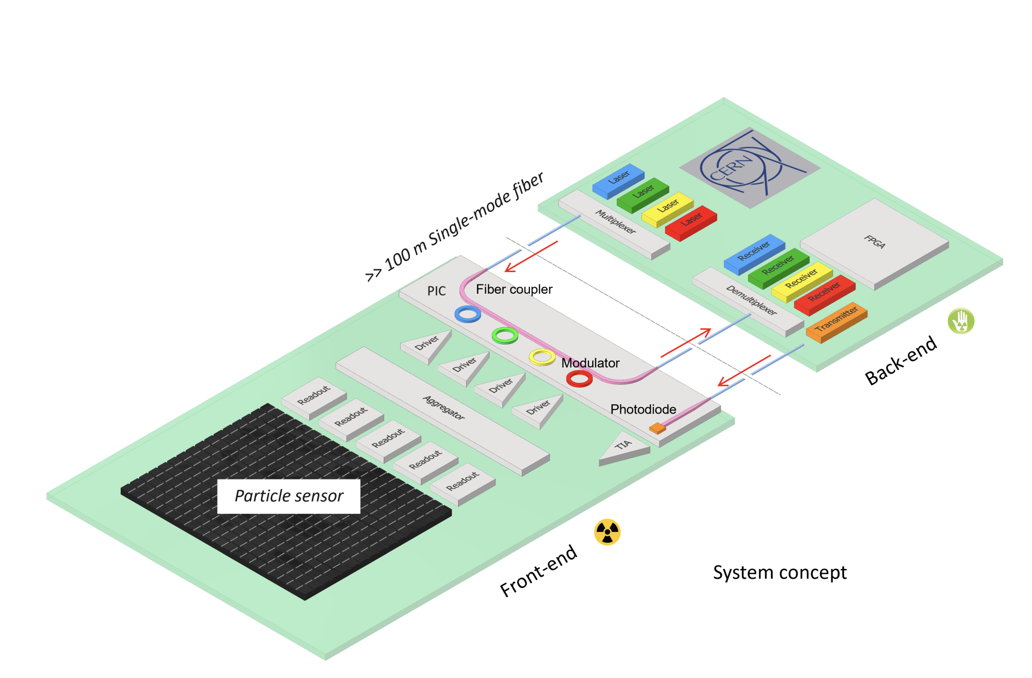
Figure 1: Concept of optical readout for particle detectors using Silicon Photonic Circuits. The front-end optical transceiver is integrated into a Silicon chiplet co-packaged with the particle sensor. Commercial off-the-shelf (COTS) optical components are deployed at the back end, a radiation-free zone.
Figure 2 a) shows the SystemPIC, which represents the third generation of test PICs taped-out by CERN and fabricated using the imec iSiPP50G technology in a multi-project wafer (MPW) run. The SystemPIC is a test vehicle for evaluating the radiation tolerance of the technology and for demonstrating the optical link concept illustrated in Figure 1. To efficiently convert electrical signals into optical signals at high speed, we use RMs, which are compact optical devices with a radius of less than 10 μm [7]. These modulators use resonance effects to modulate light supplied by external laser sources. Figure 2 c shows a wide open optical eye diagram produced by a ring modulator when driven by a 25 Gb/s electrical data signal.
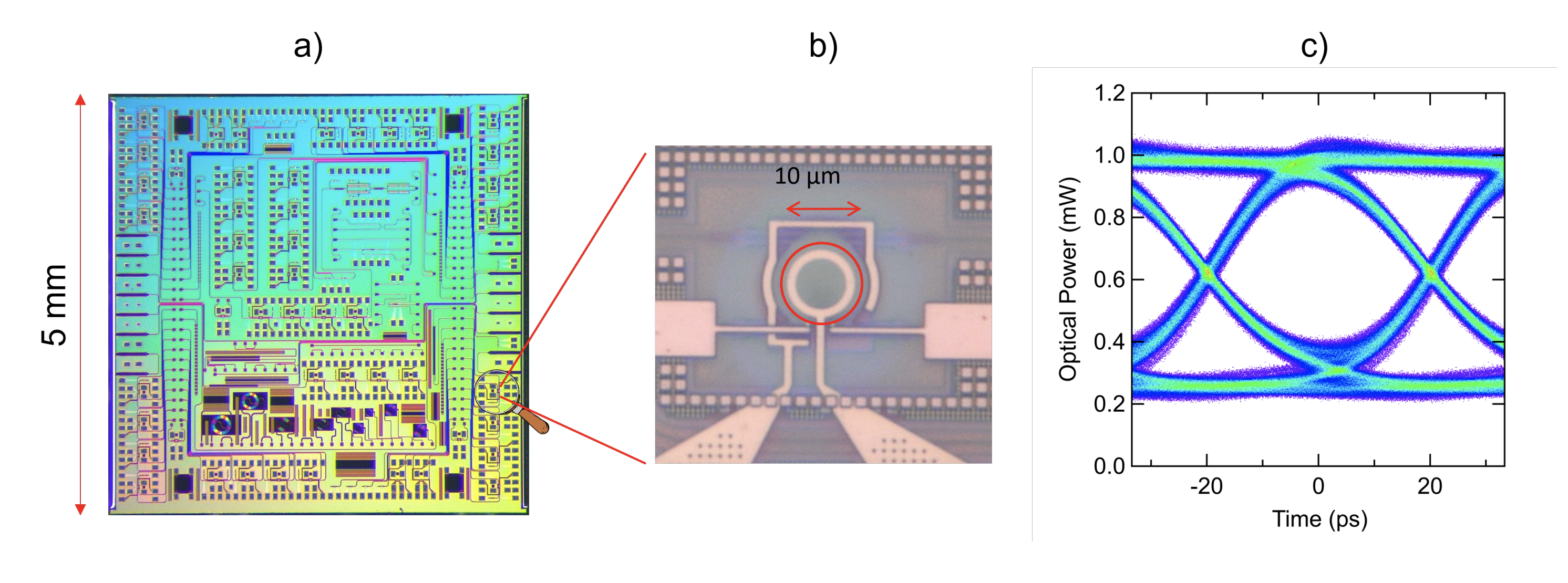
Figure 2: a) Picture of the SystemPIC, a Silicon Photonics integrated circuit designed at CERN and fabricated in the imec iSiPP50G technology. b) Micrograph of a ring modulator. c) Optical eye diagram at 25 Gb/s of a ring modulator when driven by a 2 V peak-to-peak amplitude modulation voltage.
In the EP R&D WP6 project, we developed a Demonstrator ASIC for Radiation Tolerant Transmitter in 28 nm CMOS technology (DART28) [12]. This ASIC includes data aggregation functionalities along with a 4-channel 25 Gb/s ring modulator driver circuit. We built a demonstrator to validate the concept of co-packaging the SiPh optical transceiver with the sensor readout circuit, which is emulated in this demo by the DART28. Figures 3 a) and b) show two photographs of the assembly, where the SystemPIC appears as an optical chiplet mounted adjacent to the high-speed outputs of the electronic ASIC. The high-speed interconnection between the two chips was realised in the EP-ESE labs through standard 25 µm wire bonds. To minimise the parasitic inductance, the wire bond length is reduced to approximately 500 µm. Figure 3 c shows a wide optical eye diagram at 25.6 Gb/s acquired on this demonstrator.
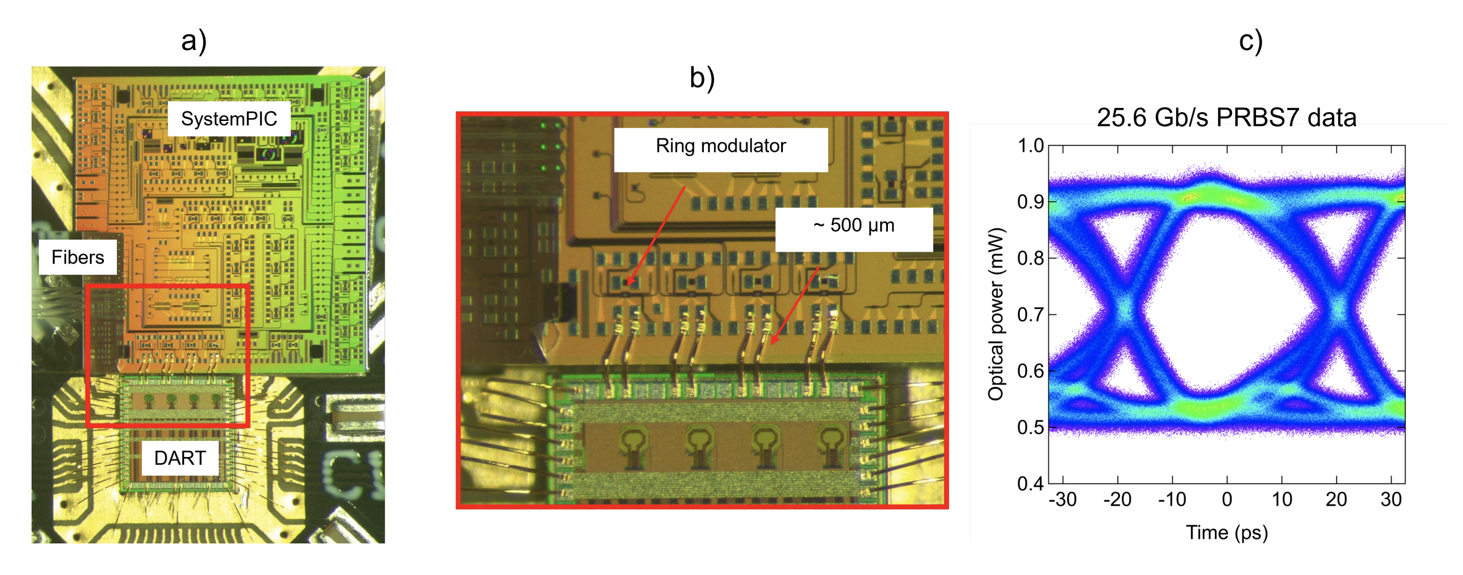
Figure 3: a) and b) Co-packaging of the SystemPIC with the CMOS quad modulator driver DART28. c) A wide-open optical eye diagram was measured on this demonstrator.
Mastering the integration of PICs with front-end particle sensors is essential for the successful adoption of SiPh in future CERN detector optical readout systems. However, standardisation of fibre optic connections to PICs is still in its infancy. To advance in this area, the EP-ESE Group strategically invested in an R&D fibre attachment machine for PICs thanks to EP R&D Funds. This piece of equipment offers substantial flexibility, allowing users to develop fully automated processes for specialised applications via a graphical user interface (GUI). The initial fibre alignment step uses image recognition techniques for a coarse positioning of the fibre array relative to the PIC. This preliminary alignment enables “first light” coupling into the PIC. Given the small core diameter of single-mode fibres and SiPh waveguides, the required alignment tolerances are in the submicron range, which exceeds the resolution of vision systems. To achieve the necessary precision, the machine employs active alignment algorithms to optimise the optical power coupling into the PIC by precisely adjusting the fibre position. Once aligned, the fibre is permanently attached to the PIC using UV-cured epoxy, applied through an automated dispensing system. The fully automated process takes about 5 minutes. The video below shows in real time the main steps of the fibre attachment to PICs.
The EP R&D initiative has significantly advanced the development of radiation tolerant data links based on Silicon Photonics, showing that this technology has excellent potential to move from a lab proof of concept to real applications. In 2024, we completed extensive irradiation and characterisation tests on both the SystemPIC and the DART28. These data sets will drive the design of a new generation of electronic and photonic test chips aiming to improve performance, radiation tolerance, and their integration with sensor ROCs.
References
- S. Shekhar, et al., Roadmapping the next generation of silicon photonics, Nature Communications, 15, (2024) 751
- J. Troska, et al., Radiation tolerant optoelectronics for high energy physics, Nuclear Instruments and Methods in Physics Research Section A, 1052, (2023) 168208
- G. Aglieri Rinella, et al., Strategic R&D Programme on Technologies for Future Experiments, CERN-EP-RDET-2024-001
- T. Prousalidi et al., Towards optical data transmission for high energy physics using silicon photonics, 2021 JINST 17 C05004
- C. Scarcella et al., System development of silicon photonics links for CERN experiments and accelerators, 2023 JINST18 C03002
- T. Prousalidi et al., System Development of Radiation-Tolerant Silicon Photonics Transceivers for High Energy Physics applications, IEEE Trans. Nucl. Sci. 70 (2023) 2373
- Y. Ban et al., Highly Optimized O-band Si Ring Modulators for Low-Power Hybrid CMOS-SiPho Transceivers, Optical fibre Communications Conference and Exhibition (OFC) (2023)
- M. Zeiler et al., Radiation Damage in Silicon Photonic Mach–Zehnder Modulators and Photodiodes, IEEE Trans. Nucl. Sci. 64 (2017) 2794
- A. Kraxner et al., Investigation of the Influence of Temperature and Annealing on the Radiation Hardness of Silicon Mach–Zehnder Modulators, IEEE Trans. Nucl. Sci. 65 (2018) 1624
- M. Lalović et al., Ionizing Radiation Effects in Silicon Photonics Modulators, IEEE Trans. Nucl. Sci. 69 (2022) 1521
- L. Olanterä et al., Effects of High Fluence Particle Irradiation on Germanium-on-Silicon Photodiodes, IEEE Trans. Nucl. Sci. 71 (2024) 728
- A. Klekotko et al., A Radiation-Tolerant 25.6-Gb/s High-Speed Transmitter in 28-nm CMOS With a Tolerance of 1 Grad, IEEE Trans. Nucl. Sci. 71 (2024) 2124