![]()
Spotlight on Hybrid Pixel Sensors
Prelude
Making the next pivotal discovery in particle physics depends on our ability to build new experiments aiming at pushing the boundaries of energy and intensity frontiers. The process of designing and building such apparatuses often originates years before any breakthrough data can be collected. While experimental physicists are busy analysing the large amounts of data accumulated during previous LHC runs, teams working under the umbrella of the EP-R&D programme are developing breakthrough technologies. Technologies intended not only to meet the challenges of the High Luminosity LHC (HL-LHC) environment, but also to pave the way towards experiments in future facilities, such as the proposed Future Circular Collider (FCC). EP-R&D programme spans an initial 5-years period from 2020 onwards, covering detector hardware, electronics, software and detector magnets for new experiments. It also encompasses detector upgrades beyond LHC phase II. In a series of articles, we will dive into the different working groups, discussing their achievements and what lies ahead.
In this issue, we meet with the team working on “Hybrid Pixel Detectors” (WP.1.1), an extensive array of physicists sharing their unfaltering energy and determination to steer the hybrid pixel technologies into the future. Led by Paula Collins and Victor Coco, today’s team is comprised of Vangelis Gkougkousis, a senior CERN fellow and one of the first members of the team, together with Jakob Haimberger from Technical University of Vienna and Marius Halvorsen from University of Oslo, joining as CERN Doctoral Students. The team was enriched in 2022 with Eloi Pazos Rial, a technical student studying in Universidade de Santiago de Compostela. The fifth member, Mohammadtaghi Hajheidari, just joined as a senior fellow, starting his contract last October.
Gkougkousis welcomes me in their laboratory, where they devise most of their setups and measurements in building 20/R-016. He highlights the key goals of the team efforts: “Looking into the future of hybrid silicon sensors for particle physics experiments means addressing a threefold challenge: high radiation fluence (>1017 neq/cm2), extreme hit rate (10 Ghits/sec/cm2) which our electronics should extract in a radiation-hard environment and last but not least providing timing resolution capabilities of at least 40 picoseconds.
But the team is not discouraged by the arduous task. “Everything comes down to asking the right questions to one another,” Gkougkousis added. “We want to know what’s possible and what’s not, work together to define the requirements in a realistic way”. To meet this goal, four alternative technologies are currently considered, namely planar pixel sensors, 3D sensors, LGADs and an innovative 3D type approach, where gain is achieved with no implants. Let us explore the meaning of these acronyms and the merits of each approach.
Pushing the frontiers in Planar Pixel Sensors
Haimberger, who pursues a PhD on this technology, explains: “We started the prototype and design phase in 2020 with first devices arriving in 2021. They feature several sensor geometries (Timepix4, Timepix3 and TDCpix), produced in various thicknesses (50, 100, 200 and 300 μm) as we expect this parameter to be crucial for time resolution and radiation hardness”. Moreover, they included two test structures, one of 1 mm diameter, optimized for timing studies, and a larger one, with a diameter of 2.5 mm, for ease of manipulation during electrical characterization and irradiation campaigns (see Figure 1).
As one might expect, pandemic related restrictions had an impact on progress. Design, simulations and tendering went through COVID19, but the team had to wait about 18 months before first samples arrived in April 2021. Following production finalisation, sensors were irradiated, both at CERN and at Ljubljana, to fluencies of up to 1017 neq/cm2 to study the role of different thicknesses in achieving the desired time resolution and performance. Through a year-long test-beam campaign at the Super Proton Synchrotron (SPS), the team collected enough data, currently under analysis, to extensively characterise their performance.
During acceptance measurements, an interesting yet puzzling feature was discovered. Haimberger explains: “The sensors were breaking down at 50 V, independent of thickness, though similar productions were stable up to 500 V and above. This unexpected behaviour was further investigated through simulations to identify the cause. It turns out that the high p-spray doping concentration, creating high field and consequently leading to impact ionisation at the interface between the readout electrode and the p-spray”. Gkougkousis and Haimberger traveled to Paris to perform Secondary Ion Mass Spectroscopy (SiMS), in collaboration with the GeMAC group of the Université de Versailles Saint-Quentin-en-Yvelines. These measurements proved pivotal for understanding the cause of this effect and moving forward with the electrical characterization.
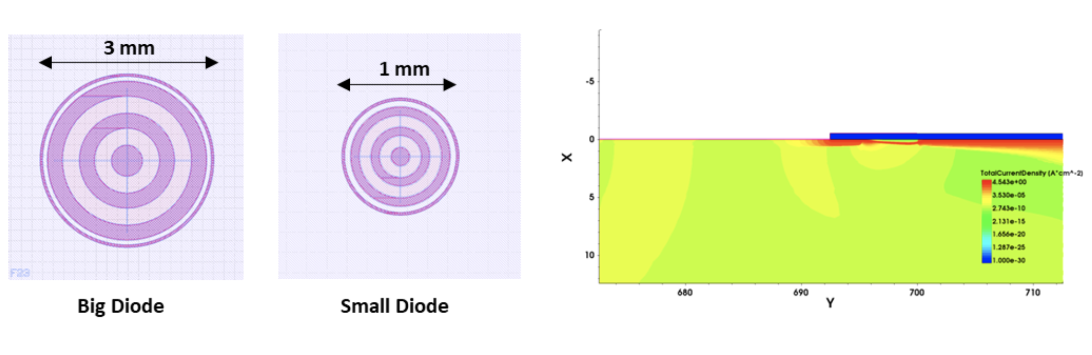
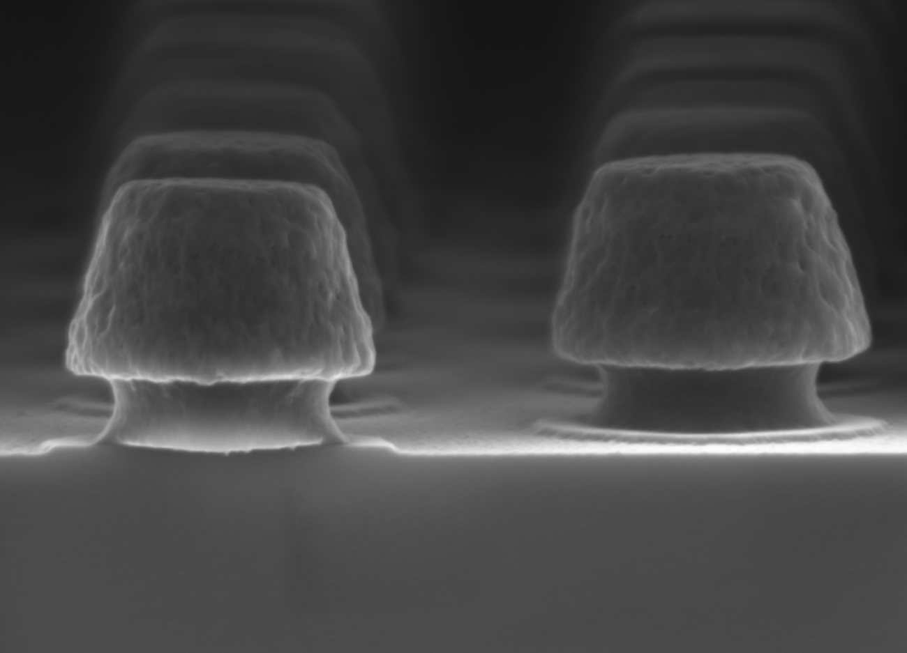
Figure 1: Part of WP1.1 activities include the systematic study of timing in planar sensors as a function of radiation and thickness. Different size circular diodes were produced, namely small for timing study (middle) due to lower capacitance and big ones (left) for radiation damage studies and simulation benchmarking (left). Plots taken from “Single cell 3D timing: Time resolution assessment and Landau contribution evaluation via test-beam and laboratory measurements”, 17th Trento workshop on advanced radiation silicon detectors.
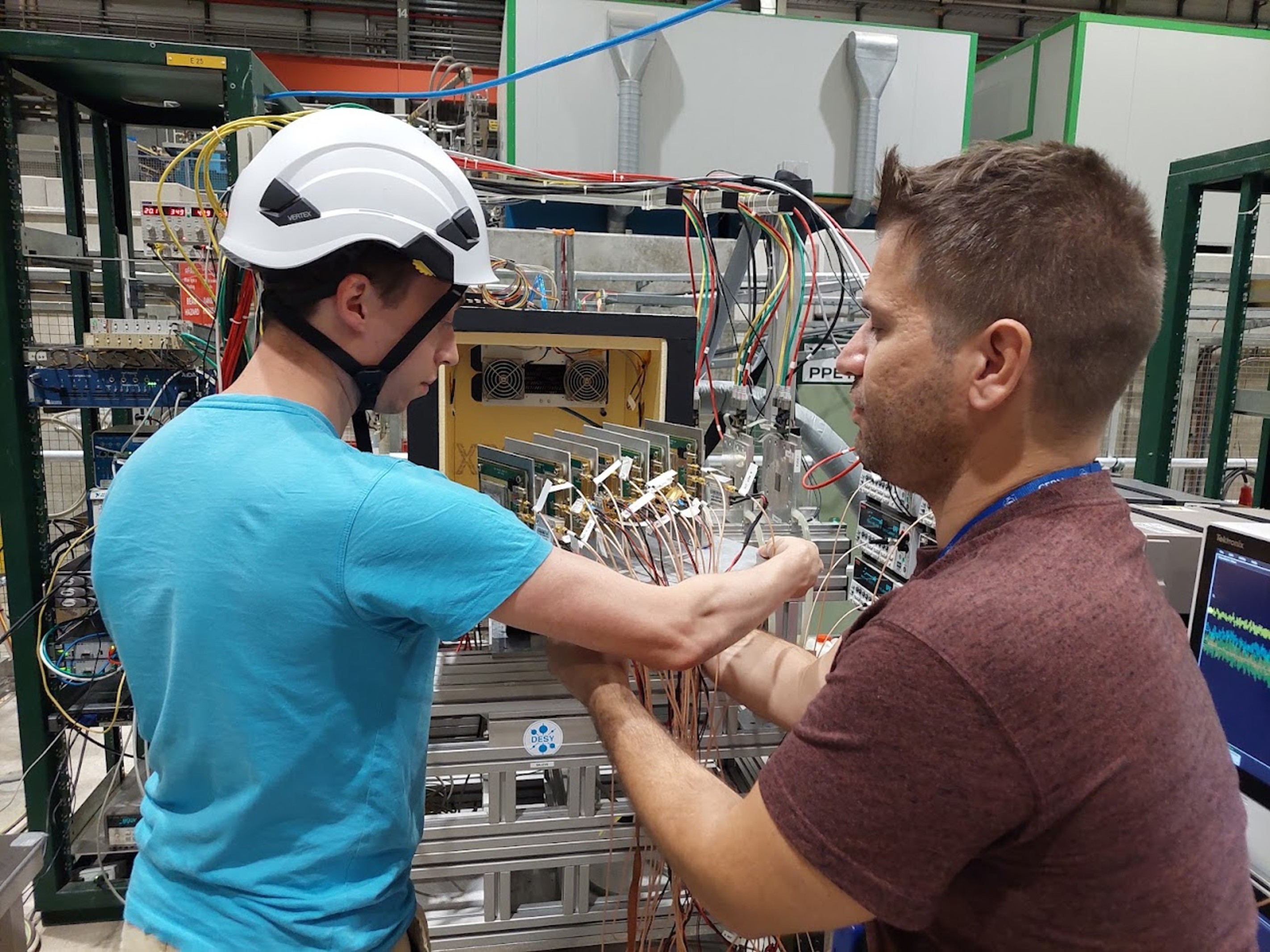
Figure 2: Vangelis Gkougkousis and Jakob Haimberger, inserting the planar pixel sensors in the beam line at SPS.
In parallel, Pazos Rial worked on extensive electrical characterization."We are running a large campaign covering different sensor thicknesses for several proton and neutron fluence points, while trying to understand whether a model can be developed describing how the behaviour of these sensors evolves during irradiation, to be used for precise simulation”. Currently, the team waits for the last irradiation step to be completed at the Proton Synchrotron (PS), closing the year-long campaign. Their tests revealed a second unexpected result: irradiated at the same fluence, the thinner sensors were producing higher currents compared to the thicker ones. It is known that when silicon sensors get irradiated, one expects higher leakage currents because of the defects induced in the crystal but they should be higher for the thicker sensors. The seemingly odd result turns out to be directly related to the high p-spray concentration in the sensor. The presence of the gain mechanism implies that due to the p-spray implant, impact ionization occurs, further increasing the measured current.
Studying the potential of 3D sensors
3D sensors have proven their potential to operate at the foreseen radiation fluences of more than 1016 neq/cm2 while achieving pitches of ~50 μm with <100 psec time resolution. “The problem with 3D sensors was that due to the pandemic and the wafer-shortage affecting the industry, there was a lack of available chips for testing” says Gkougkousis and adds “Thanks to collaboration withs CNM and IFAE in Spain, UZH Zurich and Imperial College London we succeeded to recover existing structures - produced for ATLAS/CMS experiments - and reuse them. These collaborations helped go around the chip shortage and achieve the ambitious goals we set".
The team managed to get 50 x 50, 55 x 55 and 100 x 25 μm structures, each forming a single pixel. “They were irradiated, assembled on electronics boards and inserted at the test beam to produce subpixel maps detailing the response of different pixel parts with respect to their size and thickness. The measurement campaign lasted 14 weeks this year alone, and thanks to it “we have a detailed study of both planar and 3D sensors, over the same range of fluences, without doubling the effort.” (see Figure 3).
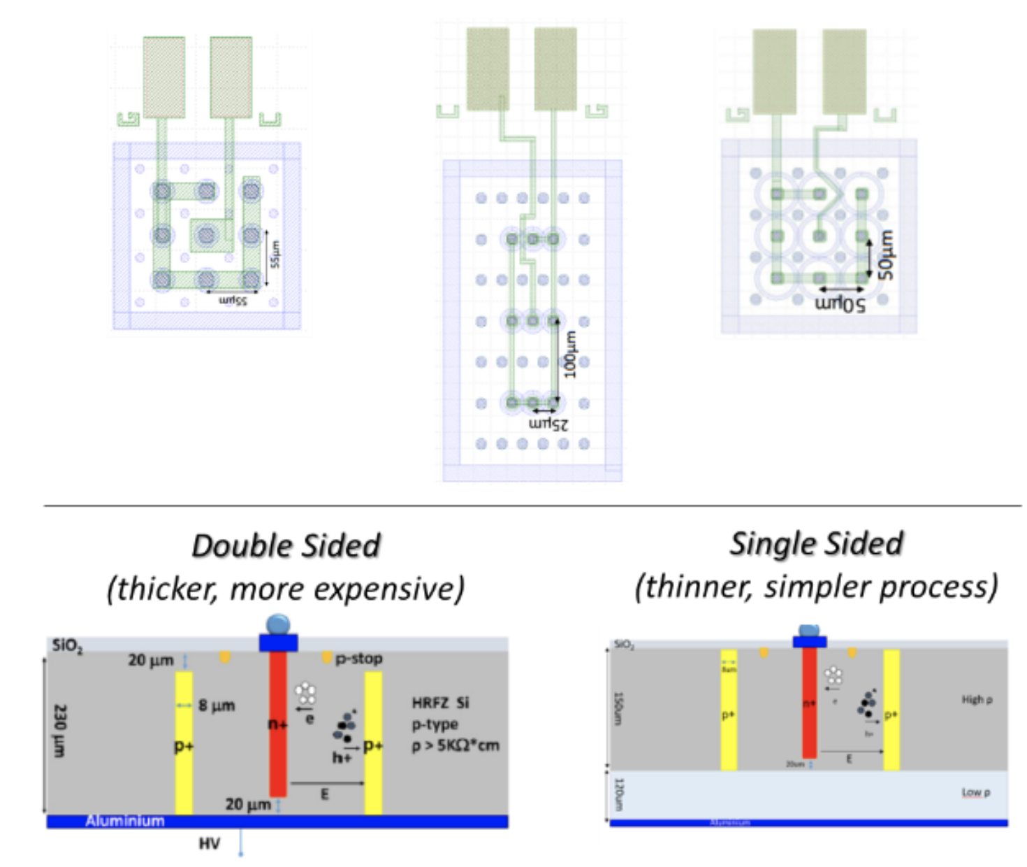
Figure 3: Structures of different thickness were used for the characterization of existing technologies for timing performances both before and after irradiation.
However, in this case there were three different geometries to be tested, based on different pixel sizes. “The idea is not only to prove whether 3D is a suitable technology or not, but also identify which is the appropriate geometry meeting the experimental requirements'”, mentions Gkougkousis. Tests started in July 2021 and finished last September, including again both proton and neutron irradiated sensors. The goal is to determine if they satisfy the needed fluence requirements of 1017 neq/cm2, and which would be the most appropriate geometry. Preliminary results show that this technology offers extremely good time resolution, close to the desired value of 40 ps (see Figure 4).
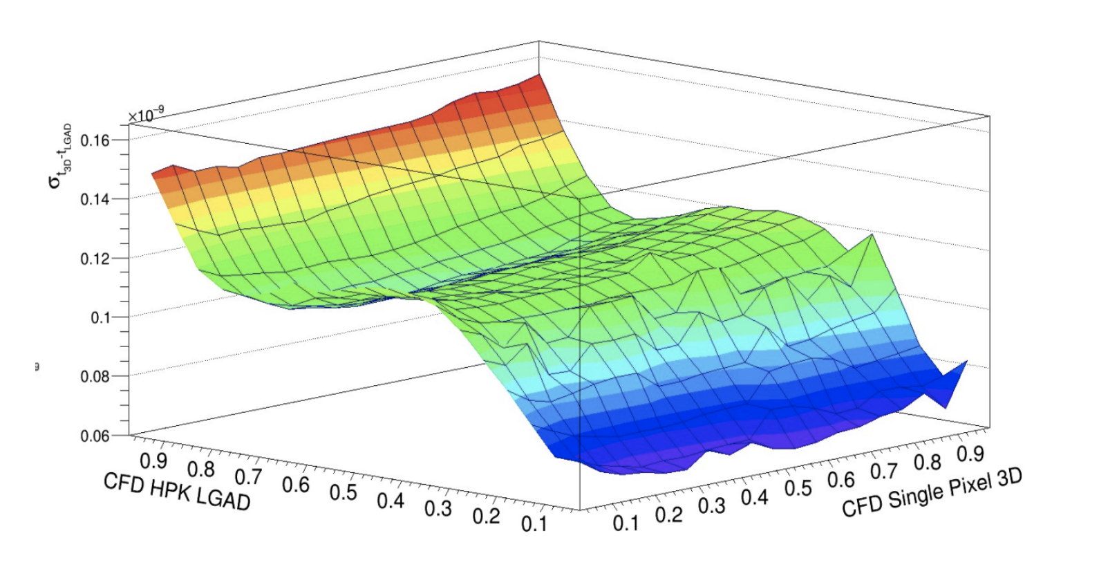
Figure 4: Map of a LGAD vs a single 3D pixel obtained at 20 V and temperature of -20 oC. Plot by V. Gkougkousis, “Single cell 3D timing: Time resolution assessment and Landau contribution evaluation via test-beam and laboratory measurements”, 17th Trento workshop on advanced radiation silicon detectors.
Given the small size of such objects, getting reliable statistics required extremely long beam time. For comparison, approximately two weeks are needed to get similar results to the ones achieved within a few hours of beam time for the planar sensors. “When it became clear that both planar and 3D sensors technology cannot be tested in a lab, we realised the need to design our own entire setup. This meant that we had to find and often build from scratch the required equipment, trying to recycle existing material and economise the use of resources”. On that note, the team refers to the role of the SPS coordinator for the efficient allocation of beam time, enabling the smooth completion of the measurements.
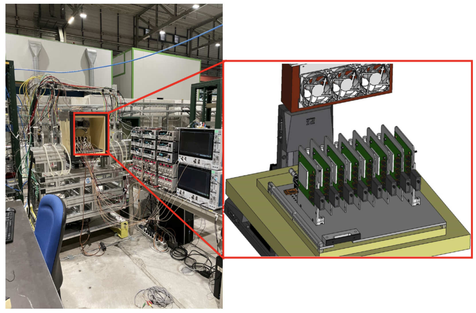
Figure 5: Cold box with sensors at the SPS North Area, ready for test beam. The versatile and automated setup allows remote operation compatible with both 3D and planar sensors. Image from V. Gkougkousis “Sensor Characterization: from process to timing” presented during the last EP-R&D days.
Furthermore, the momentum of the project has attracted new collaborators from institutes who are not part of the EP-R&D programme but participate directly in the work of WP1.1. A number of younger colleagues got involved in testing and took shifts during the summer and autumn test-beam runs at SPS.
![]()
Figure 6: Vagelis Gkogkousis, Marius Halvorsen and Efren Rodriguez Rodriguez: Late night in front of the tracking telescope testing 3D sensors at the North Area.
Test the boundaries of LGADs - Low Gain Avalanche Diodes technology
Exploring LGADs as part of previous work, allowed to think about what can be improved and whether this technology fits within the LHCb requirements. In the LGAD radiation hardness studies presented by Gkougkousis in 2020 and 2021, a 20% improvement in charge collection was established for deep carbonated substrates without noticeable effect on gain layer deactivation.
LGAD is a sensor like a planar sensor, but you have in addition a third implant as a gain layer. Gkougkousis was already exploring LGADs for the ATLAS and CMS experiments. “It was a continuation of this work which fitted well due to COVID19. We had a six month of dead time allowing us to revisit and analyse previous measurements and extract useful lessons. This also allowed us to realize the needed steps and whether this technology is promising to meet the specifications given to our WP”. Three different gain layer dopants were tested, namely gallium, boron and carbon infused boron and results were published at the Journal of Physics and Frontiers. Following these publications, we started discussing how to move forward and what is the optimum strategy to further improve this technology. The proposal was to try indium and lithium gain layers, so I ran process simulations trying to optimize the fabrication parameters. As a result of this study, an RD50 project request was approved and funded for further investigation (project RD50-2021-03). The simulations and mask design for this test-run have been completed but shortages in the global wafer market and fabrication related delays have pushed the expected arrival date of first samples towards the end of 2022”.
A new player in the game: Silicon electron multiplier sensor
A fourth innovative technology is also explored in the framework of WP1.1, based on a sensor with intrinsic gain, the Silicon electron multiplier (SiEM). As Halvorsen explains “It is challenging to combine good time resolution and radiation hardness in a single device with fine pitch” and continues “the idea resembles to an extend to the logic of LGADs. However, in SiEMs the internal gain is not achieved through doping, as in LGADs, but by burying additional electrode grids within the semiconductor substrate", as illustrated in the figure 7 below.
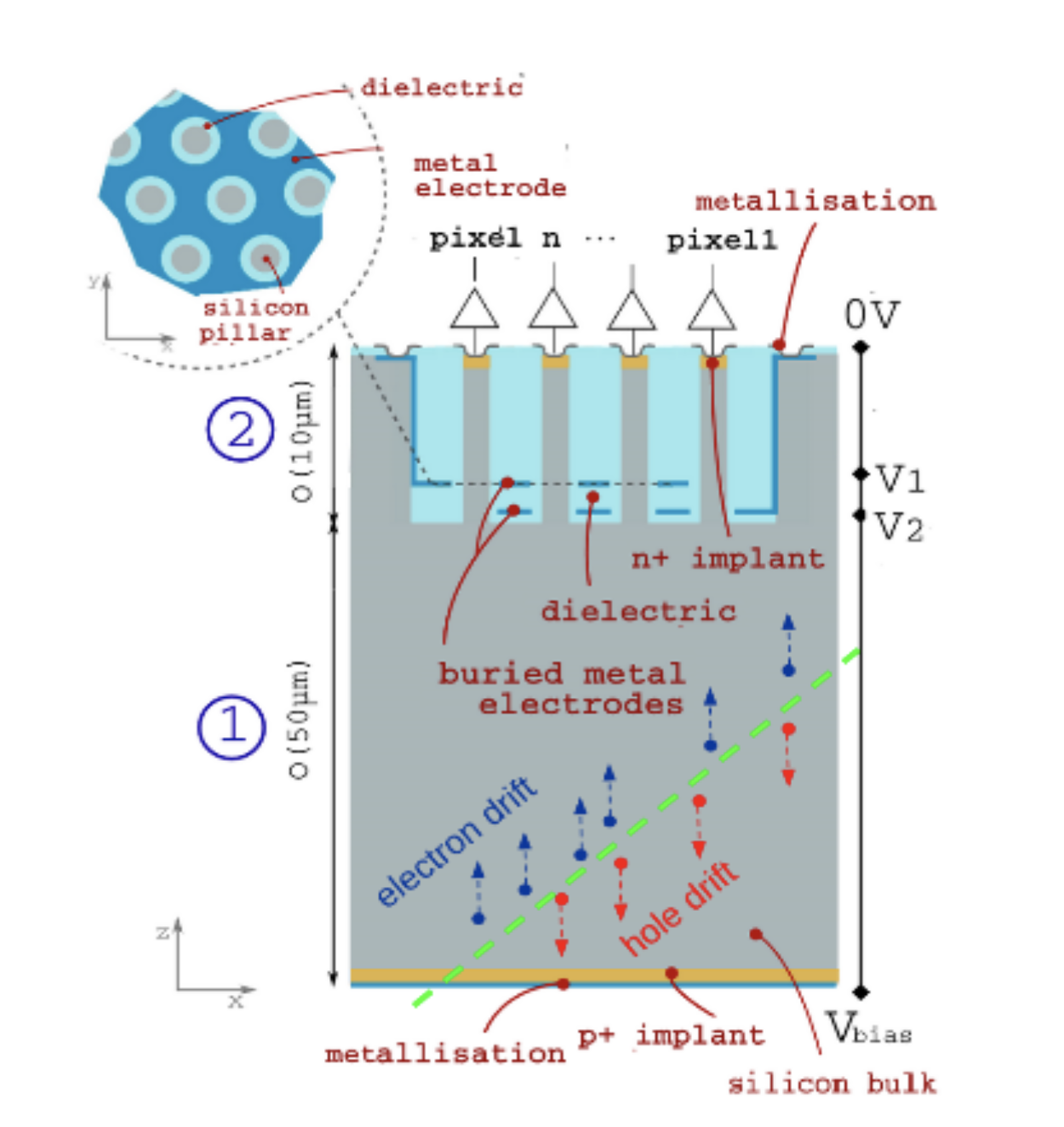
Figure 7: Basic design of the newly proposed SiEM. By implementing additional electrodes close to the readout, high electric field regions are created promoting charge multiplication. The proposed design avoids doping dependent gain regions, thus offering the potential of a radiation hard sensor with good timing capabilities. From the NiMA paper “The Silicon Electron Multiplier Sensor”.
The merit of this technology is that it can deliver good timing performances thanks to the internal gain but without suffering the radiation sensitivity observed in LGADs since it avoids the gain layer deactivation. “The problem with implants is that after irradiation they degrade, while in the SiEMs the additional electrodes should not be impacted that much”.
Results from early simulations in 2021 were rather promising, showing that amplification could be achieved as demonstrated in Figure 8, illustrating the charge multiplication. "Moving further towards fabrication, we consider two alternative processes. One is the so-called Deep Reactive Ion Etching, developed in partnership with CNM-CSIC in Barcelona and co-funded by AIDA Innova Blue Sky R&D call in 2021. The second process is Metal Assisted Chemical Etching co-developed with a team at Paul Scherrer Institute (PSI) outside Zurich".
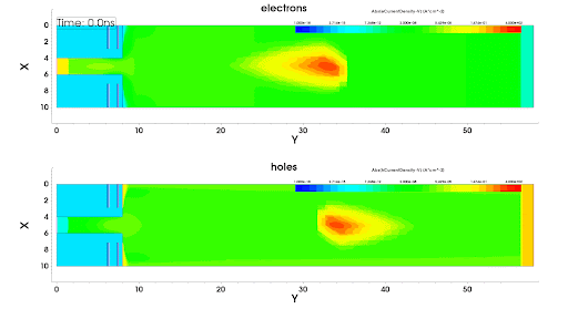
Figure 8: Example of the functionality of the SiEM for an electron-hole cloud at the middle of the structure. As electrons (top) drift towards the pilar, they encounter the high field region defined by the two lateral electrodes and multiply. At the bottom, we can thus observe two distinct “waves” of holes moving towards the cathode. The first one from the original cloud and the second one because of the multiplication. Plot taken from M. Halvorsen “Silicon Electron Multiplier (SiEM)”, 17th Trento workshop on advanced radiation silicon detectors.
This technology was applied for the first time in active media and if proved successfully, it could largely simplify the manufacturing process while meeting the key design characteristics for timing resolution and performance. As for the next steps for the study of this sensor, Halvorsen Says "We have just finished the first production using Metal Assisted Chemical Etching and are now characterising the prototypes. The first tests seem promising, but more testing is needed. Lessons learned in the first production will be implemented in a second iteration. Also, the fabrication using deep reactive ion etching is on-going, and we are very much looking forward to the outcome".
Building a Timepix4 telescope
The team has also been involved in the construction of a charge particle telescope based on Timepix4 ASIC, targeting spatial resolution down to 2 µm, track time stamping capabilities with time resolution down to 80 ps and high readout rate capabilities allowing to exploit the full SPS rate (Figure 9 left). It is based on Timepix4 readout and is a collaboration between CERN, Nikhef, USC, the University of Dortmund, the University of Oxford, IFCA and the University of Manchester. The CERN group designed the mechanics for the telescope support arms and the DUT box, including vacuum and cooling capacities. They also implemented the motion system for the telescope and DUTs.
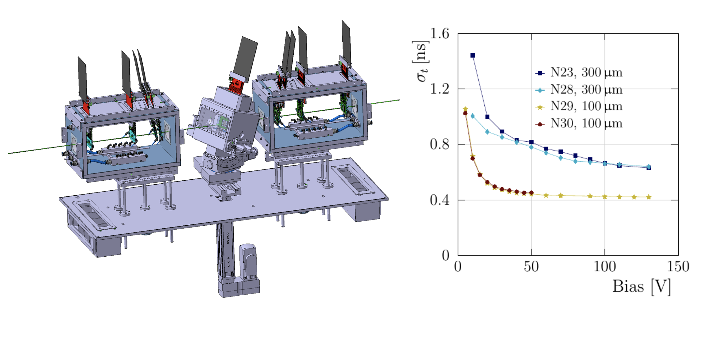
Figure 9: 3D modelling of the complete Timepix 4 Telescope (left). Two independent arms are visible with four planes per arm, while a DUT mounting enclosure is foreseen in the middle. Time resolution vs bias voltage (right) of the different thickness planar sensors achieved using the TimePIx4 ASIC.
Hajheidari has become familiar with the operation of the Timepix 4 chip. The preparation of a setup in the lab for testing this chip is ongoing. In parallel, calculations for a new production of 3D sensors have been made. “Over the past months, I did the calculations of 3D sensors capacitance that would allow achieving a timing resolution of 50 picoseconds for the sensor-readout assembly. As the resolution depends on the sensor and readout parts of the team, my work involved interaction with colleagues working on the readout electronics - trying to integrate all parameters in a unified framework”. Thanks to this work, the geometrical specifications of the 3D sensors for launching a tendering process will be defined.
Coda
As for the future, the team would like to see a choice among the different technologies. “We would like our work to provide a basis that clearly indicates the boundaries of these technologies and allow making informed decisions based on the requirements put forward by the experimental collaborations” explains Gkogkousis. The work of WP1.1. could lead to a new mixture of dopants for the LGADs based on the efforts put over the past year. For Gkougkousis “this would be something similar to the radical development of gaseous detectors that required years of development before finally establishing what is now referred to as -the magic gas- the ideal gas recipe for particle detection and sensor stability”. Furthermore, SiEM technology holds a great potential for future detector sensors combining excellent timing capabilities with fine pitch and radiation hardness. Halvorsen envisions a full-blown production giving results verifying the obtained gain in time resolution and finding its way in the detectors considered for future accelerators.
To meet these goals, the team will continue actively collaborating with many universities and research centres around the world. Their work plan is tightly linked to the work done in other Work Packages of the EP-R&D Programme while also exploring links with other R&D initiatives such as RD50 and AIDA-innova (Timepix4 planes for EUDET telescope, iLGAD production, SiEM production). Collaborations with other institutes’ R&D include Nikhef, CPPM, UCSC, University of Oxford, ETH & EZH Zurich and PSI as well as cross-talks with experimental upgrades planned for LHCb and NA62.
A visit to their lab will convince you about the ingenuity and creativity that it takes to reach these milestones during these turbulent times. The interest triggered by academic partners and the links developed with industry, is not only rewarding but also reassures about the validity of the adopted approaches. Hopefully the outcome of this work could provide the right tools for exploiting the physics potential of the LHC and future colliders, thus paving new ways in the search for new physics beyond the Standard Model of particle physics.
Further Reading
3D Pixels Conference Presentations
17th Trento Workshop (March 2022): https://indico.cern.ch/event/1096847/contributions/4743685/
15th Pisa Meeting on Advanced Detectors: https://agenda.infn.it/event/22092/contributions/166722/attachments/90864/123094/3DPixel_Poster_PISA22.pdf
LGAD Conference Presentations
TIPP2021 (May 2021): https://indico.cern.ch/event/981823/contributions/4293572/
Zurich Pico-Second Workshop (September 2021): https://indico.cern.ch/event/861104/contributions/4514659/
EP-R&D Seminar (July 2021): https://indico.cern.ch/event/1054861/
17th Trento Workshop (March 2022): https://indico.cern.ch/event/1096847/contributions/4742738/
16th Trento Workshop (March 2022): https://indico.cern.ch/event/983068/contributions/4223170/ (Lithium, Indium RD50 Project)
SiEM Conference Presentations
iEEE NSS MIC (October 2021): https://www.eventclass.org/contxt_ieee2021/scientific/online-program/session?s=31#e222
17th Trento Workshop 2022 (March 2022): https://indico.cern.ch/event/1096847/contributions/4743677/
EP-R&D Seminar (April 2022): https://indico.cern.ch/event/1139247/
CEPC Workshop (October 2022): https://indico.ihep.ac.cn/event/17020/contributions/118940/
Articles
E.L. Gkougkousis et al., « Comprehensive technology study of radiation hard LGADs”, https://iopscience.iop.org/article/10.1088/1742-6596/2374/1/012175, 2022 J. Phys.: Conf. Ser. 2374 012175
M. Halvorsen et al., “The Silicon Electron Multiplier Sensor”, NIMA, Vol. 1041, 167325, October 2022, https://doi.org/10.1016/j.nima.2022.167325
E. L. Gkougkousis et al., “Tracking the Time: Measurements towards the characterization of a 3D pixel in terms of time resolution and Landau contribution evaluation”, NIMA, Volume 1047, February 2023, 167788