![]()
Sub 25-ps timing with PICOSEC Micromegas gaseous detectors
Precise timing systems are central to many ongoing and planned detector upgrades and tens of ps timing resolution will play an important role to meet detection challenges in future high-luminosity environments. Large area detection systems achieving such timing resolution can offer unprecedented precision in particle tagging and superior pile-up mitigation potential and enable new experimental possibilities. While gaseous detectors are a well-established technology for large-scale tracking systems and are already employed as well as being implemented in upgrades of LHC experiments, they were typically limited in achievable timing resolution on the order of nanoseconds. The PICOSEC Micromegas concept overcomes this limitation and offers a scalable solution with excellent timing precision with gaseous detector technology at the level of 25ps. In addition to time tagging and tracking of collision products, this development can provide event-level monitoring of neutrino beams in the context of the ENUBET NP06 project at the CERN Neutrino Platform [1], allow precise timing in electromagnetic calorimeters and be used as a performant photon detector for systems including Detection of Internally Reflected Cherenkov light (DIRC) detectors.
The time resolution of conventional gaseous detectors is limited by uncertainties in the location of primary ionisation in the sensitive detection volumes, with a typical thickness on the scale of millimetres. Due to low density of gas as an active medium, the thickness of these conversion volumes cannot be significantly decreased thus limiting achievable timing jitter to the level of nanoseconds. Gaseous detectors based on MicroPattern Gaseous Detector (MPGD) technologies such as Gaseous Electron Multipliers (GEMs) or Micro-Mesh Gaseous Structures (Micromegas) usually use low-field drift regions to transport primary electrons to an amplification stage where avalanche multiplication occurs in high electric field regions. In the case of Micromegas, high electric fields are formed by a potential difference between a micro-mesh and an anode electrode with a separation of typically 128µm. The micro-mesh is supported by pillars formed by photolithography to define a uniform amplification gap thickness. Micromegas are used in various experiments and applications and large-area resistive Micromegas are integrated in the ATLAS New Small Wheel upgrade.
To overcome the timing limitations of conventional gaseous detectors, the PICOSEC Micromegas detectors use a Cherenkov radiator to produce prompt Cherenkov light emission as a signature for traversing particles as shown in figure 1. The Cherenkov light is then converted to electrons on a semi-transparent photocathode layer coated on the radiator crystal itself. This leads to the prompt and synchronous production of photoelectrons at the photocathode and ensures that all electrons originate at a well-defined location. Subsequently, avalanche multiplication in high electric fields in the gas gaps between the photocathode, a micro-mesh and the anode is used to multiply electrons and induce detectable electronic signals.
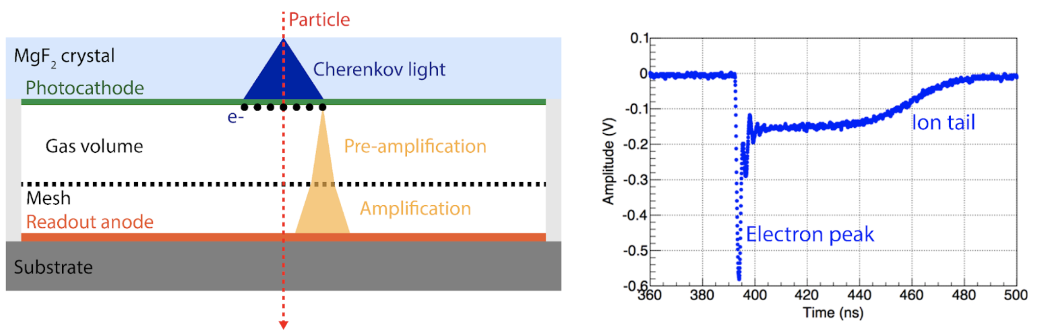
Figure 1. PICOSEC Micromegas detector concept consisting of Cherenkov radiator crystal coated with semi-transparent photocathode and two-stage Micromegas amplification stage operated in a Ne + C2H6 + CF4 (80/10/10%) gas mixture at ambient pressure (left). Typical signals exhibit electron peak and ion tail (right).
First proposed in 2015, excellent timing resolution was achieved with the first small-area prototype detectors and the concept was advanced by the developments of the PICOSEC Micromegas collaboration and in the context of an RD51 Common Project. Time resolution values as good as σ = 24ps for single Minimum Ionising Particles (MIPs) were measured in test beam campaigns at the CERN SPS H4 beam line, demonstrating the advantages of this detection concept [2]. Extensive R&D efforts were conducted by the involved institutes including among others CEA Saclay, AUTH, USTC and the EP-DT-DD Gaseous Detector Development (GDD) team at CERN to fully exploit and optimise the performance of PICOSEC Micromegas detectors.
In contrast to conventional gaseous detectors, PICOSEC Micromegas use high electric fields in both gaps to create a so-called pre-amplification region in the 200µm gap between the photocathode and the mesh and an amplification region in the 128µm gap between the mesh and the readout anode. A significant step in understanding the inherent limits of the technology and physical processes dominating time resolution was the development of a microscopic simulation framework that could reproduce experimental observations [3]. A dependence of the signal arrival time and the time resolution on the signal charge could be explained by the onset of avalanche multiplication in the pre-amplification region thus explaining the benefit of high electric fields in both regions. An early onset of multiplication in the pre-amplification region leads to both longer avalanches and thus higher signal charge as well as earlier signal arrival times as electron movement is faster during avalanche multiplication as shown in figure 2. This dependence could be reproduced by simulations and is now driving the design of prototypes with thinner gaps and possibly high electric fields between photocathode and mesh. Time resolution values below 20ps for MIPs were achieved with prototypes with pre-amplifications gaps with only 120µm thickness.
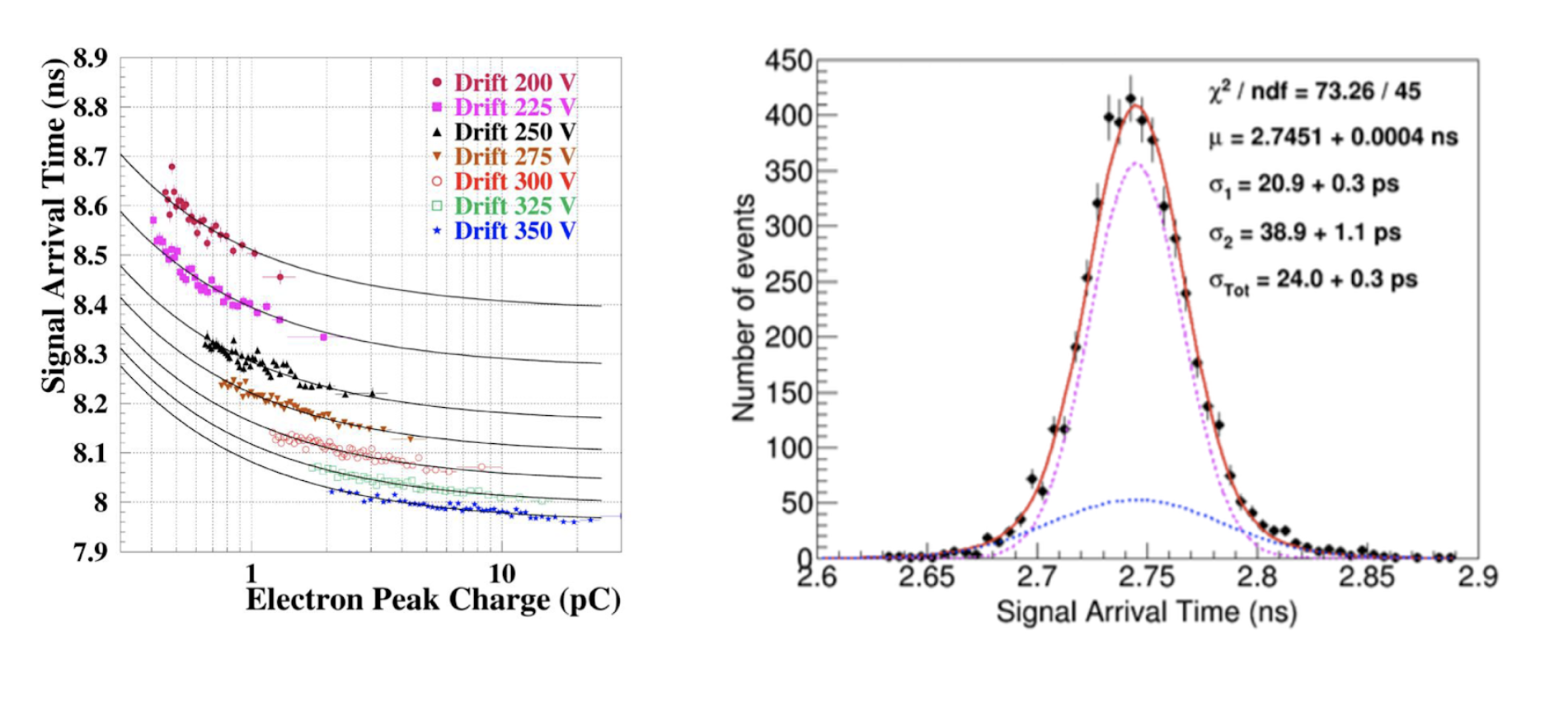
Figure 2. Signal arrival time decreases for larger electron peak charges. This reflects the faster movement of electrons during multiplication in the pre-amplification gap (left). Distribution of signal arrival time (PICOSEC signal relative to MCP-PMT reference) to measure time resolution (right). Figures taken from [3].
Scaling precise timing gaseous detectors based on PICOSEC Micromegas to larger area coverage with moderate spatial information requires preservation of timing performance when using segmented anode pads and reading out signals shared across multiple pads. The Cherenkov light produced in the radiator is spread over an area with a radius close to the thickness of the crystal, i.e. 3mm for most prototypes. When hitting the photocathode, this will create electrons over a circular area which are then amplified in the two following gaps. In a detector with segmented readout anode, multiple photoelectrons from a single particle can be either collected in a single pad or shared between adjacent pads, depending on hit location and pad size. To evaluate the effect on timing resolution, multi-pad PICOSEC prototypes with hexagonal and square anode pads with dimensions of approximately 1cm x 1cm were built. A beam telescope consisting of three GEM-based tracking layers was used to provide a reference location for crossing MIPs in SPS H4 test beam campaigns and the response of multi-pad PICOSEC prototypes was studied for signals fully contained in a single pad or signals shared between two to four neighbouring readout pads. When each pad only receives a part of the total signal charge, the fraction in each pad must be taken into account to correct for time walk and accurately combine the information from multiple pads to a single time of arrival measurement for the event. The obtained combined time resolution for multi-pad hits was shown to be around 32ps for a hexagonal pad prototype and thus only slightly worse than for single-pad hits [4].
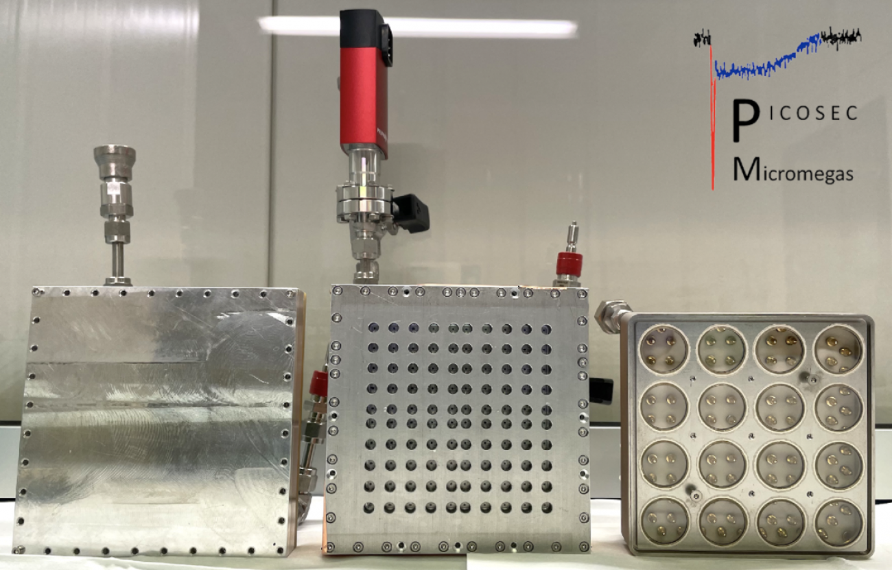
Building on the experience from first multi-channel PICOSEC prototypes, tileable 100-channel detector modules with an active area of 10cm x 10cm were developed. For this larger area, uniform thickness of the pre-amplification gap of the detector was crucial and required careful optimisation of the manufacturing process of the Micromegas at the EP-DT MicroPattern Technologies workshop. The flatness of a hybrid ceramic+FR4 substrate was closely monitored on the micrometer level with a 3D microscope during all steps of the production process, from substrate preparation to polishing, patterning and integration of the micro-mesh and pillars to form the Micromegas amplification structure and a strategy to achieve better than 10µm planarity across the active area was identified as shown in figure 3 and described in [5]. PICOSEC detector modules were studied in test beam campaigns in 2021 and could achieve around 25ps precision across the active area without the need for geometric corrections based on an external tracker. This shows that the level of uniformity of the detector response is suitable to achieve high timing precision across the 10cm x 10cm active area.
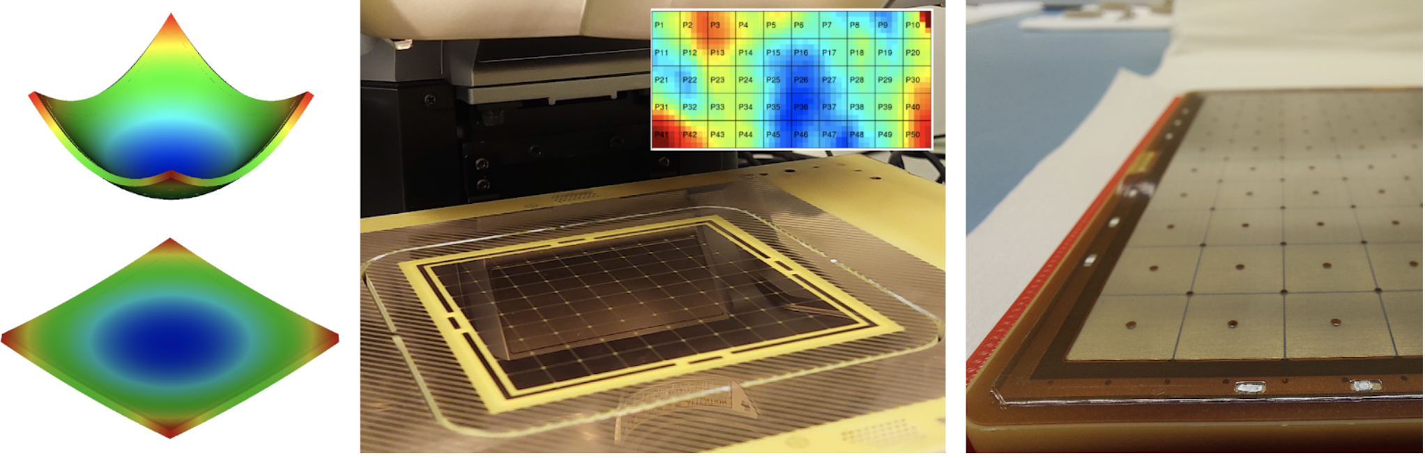
Figure 3. Mechanical simulations were used to choose a rigid substrate with minimal deformation caused by the tension of the Micromegas mesh (left, A. Utrobicic). The uniformity of the Micromegas substrate (inset) was monitored during production with a 3D microscope (center). When <10µm planarity was reached with successive polishing steps, the micro mesh was fixed to the board and pillars were defined during the bulking process (right).
The tested prototypes were integrated in custom housings with connections and services located in the back for 4-side tileability as shown in figure 4. To increase possible fill factors and minimise dead space between modules, a more compact sealed detector module is being developed with the support of F. Motschmann and colleagues from EN-MME. This Ti-housing uses hermetic sealing techniques including brazing and electron beam welding to avoid o-rings and minimise the space needed for the encapsulation of the detector. In addition, the use of low-outgassing components including a ceramic-based detector substrate, a ceramic board with brazed feedthrough-pins and metallic housing and gas filling components aims at prolonged operation in sealed mode without the need for continuous gas renewal or flushing.
While single-channel prototypes were read out with proprietary high-bandwidth preamplifiers and oscilloscopes, scalable readout electronics are required to profit from the time resolution of 100-channel detector modules or future larger PICOSEC detectors. Multiple readout electronics approaches are being explored including custom fast preamplifiers developed by P. Legou and colleagues at CEA Saclay, charge-sensitive preamplifiers with inherent time-walk correction (H. Müller) and ASIC-based options. First beam tests with custom preamplifier cards plugged into the back of multi-pad PICOSEC modules (figure 4 right) show promising performance. In addition, digitisation with SAMPIC waveform digitiser modules is explored and was shown to reproduce good timing performance despite a slightly reduced sampling rate.
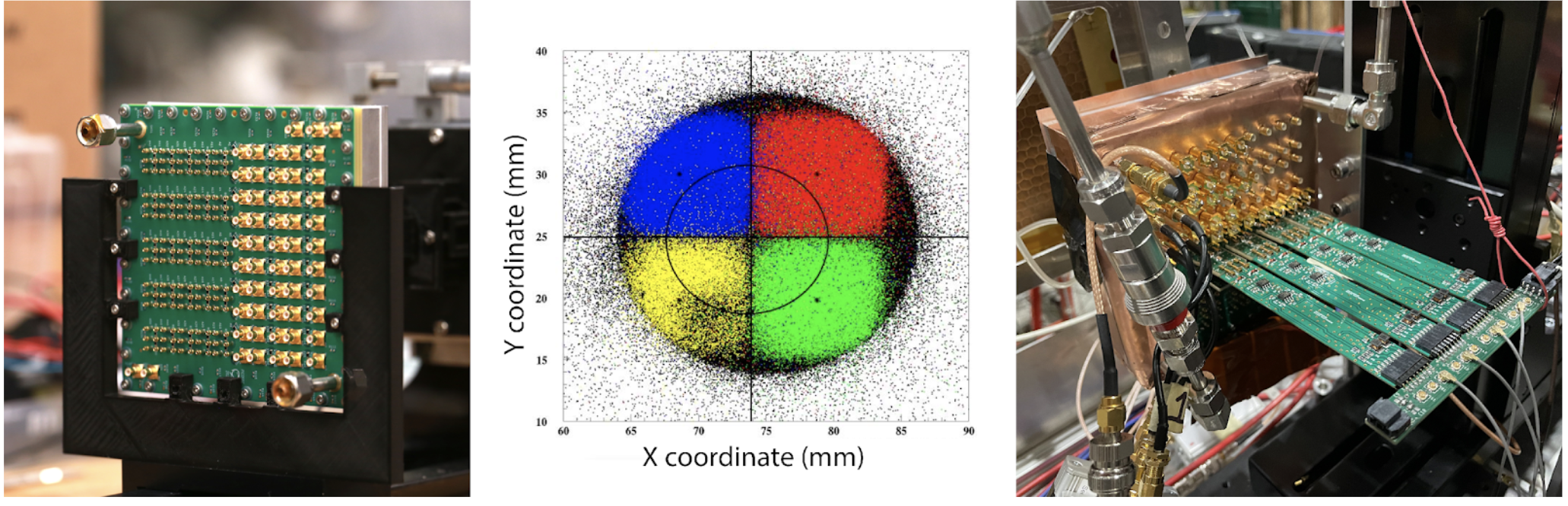
Figure 4. Tileable multi-pad PICOSEC modules were tested in lab and test beam campaigns (left, A. Utrobicic). Signals shared between four readout pads are used to measure time resolution for particles crossing between pads (center, A. Kallitsopoulou, I. Maniatis et al., AUTH). Custom preamplifier cards mounted to PICOSEC module during test beam run (right, P. Legou, IRFU CEA Saclay).
The achievable timing resolution of PICOSEC Micromegas detectors is closely related to the performance of the photocathode where primary electrons are produced from the Cherenkov light emitted in the radiator crystal. Highest time resolution values were obtained with semi-transparent photocathodes on MgF2 crystals consisting of a 3nm thick Cr layer for adhesion and electrical contact and a 18nm thick CsI photocathode layer produced by physical vapour deposition by M. van Stenis and colleagues in the EP-DT Thin Film and Glass Lab. While CsI offers high quantum efficiency (QE) for Cherenkov light and produces more than 10 photoelectrons per MIP, it is susceptible to degradation when exposed to humidity, excessive light intensity or when bombarded with ions. While exposure to humidity can be minimised with precautions during detractor assembly, ions created during avalanche multiplication in the Micromegas gain stage will reach the photocathode and significantly degrade its performance over time with more than 90% degradation in QE observed for accumulated charges of tens of mC/cm2.
While some low-rate applications may be able to operate with CsI maintaining good QE over time, high-rate environments require more robust photocathodes to preserve the tens of ps precision provided by PICOSEC detectors. Possible solutions to overcome this limitation are the use of alternative photocathode with inherent robustness against ion bombardment or the encapsulation and protection of CsI with thin layers which can block ions while preserving high photoelectric extraction efficiency. Multiple alternative photocathode materials including Diamond-Like Carbon (DLC), Boron Carbide (B4C) and metallic photocathodes (Al, Cr) were tested and while both DLC and B4C provide only about one third of the number of photoelectrons compared to CsI, they are insensitive to humidity and also appear to be significantly more robust against ion bombardment. To quantify the performance and robustness of alternative materials, the dedicated photocathode ageing characterisation facility ASSET shown in figure 5 was built in the GDD lab starting from a previous evaporation and characterisation facility. In addition to validating the above-mentioned possible alternatives, this setup is used to explore novel photocathode materials including nanodiamond photocathodes and photocathode developments profiting from low-dimensional materials and nanostructures in the context of a project within the CERN Quantum Technology Initiative (QTI).
Figure 5. The dedicated photocathode characterisation and ageing facility ASSET was built in the GDD lab to study the robustness of CsI, DLC and B4C photocathodes as well as potential alternatives (M. Lisowska).
In addition to photocathode robustness, long-term operation of PICOSEC detectors requires stable Micromegas amplification stages which are robust against possible discharges. Resistive Micromegas technology is successfully applied to minimise the potential damage from discharges and is widely used including the Micromegas detectors for the ATLAS New Small Wheel upgrade. The effect of resistive anodes on the timing performance of PICOSEC detectors was investigated for different resistive readout schemes and resistivity values. While timing performance of resistive prototypes was slightly worse compared to non-resistive detectors, prolonged operation in intense Pion beams was possible without destructive discharges. Resistive PICOSEC detectors are currently studied experimentally and through dedicated simulations (D. Janssens, [6]) not only for their protective mechanism but also for the possibility to exploit signal sharing across multiple readout pads for improved spatial resolution.
The intensive and diverse R&D programme on numerous aspects of PICOSEC Micromegas detectors over the past years has explored a wide range of technologies and possibilities for optimisation and adaptation of this technology for different applications. The 10cm x 10cm tileable detector modules with uniform timing response of approximately 25ps across the active area demonstrate the potential for large area timing systems based on this approach. Along with the development of custom readout electronics and the improvement of timing resolution below 20ps with thin gap detectors and the R&D into photocathodes and resistive Micromegas, this demonstrates the possibility to adapt the detection concept to harsh operating environments and challenging conditions.
Future developments will focus on profiting from resistive readout schemes for improved spatial resolution, increase the achievable fill-factor with larger 20cm x 20cm active area detector modules and explore alternative readout approaches preserving the excellent timing precision of the detectors. The range of possible application-specific optimisations such as detector granularity, resistivity, photocathode options and readout electronics illustrates the flexibility of the PICOSEC Micromegas technology for precise timing with gaseous detectors.
Acknowledgments
PICOSEC Micromegas are a development of members of the PICOSEC Micromegas collaboration: https://picosec-mm.web.cern.ch
Developments in the EP-DT-DD Gaseous Detector Development (GDD) lab at CERN are supported by the EP strategic R&D programme on Experimental Technologies.
We thank the RD51 collaboration for the opportunity to test PICOSEC Micromegas detectors during RD51 test beam campaigns in the SPS H4 beam line and gratefully acknowledge the support of SPS and EHN1 teams during test beam campaigns. Furthermore, we would like to thank our colleagues from EN-MME & EP-DT-EO for support with the sealed detector housing, M. van Stenis and T. Schneider from the Thin Film and Glass (TFG) lab for detector mechanics and test setups as well as photocathode preparation and Rui De Oliveira and colleagues at the MicroPattern Technologies (MPT) workshop for integrating Micromegas detectors and optimising detector production processes.
References
PICOSEC Micromegas project: https://picosec-mm.web.cern.ch
[1] A. Longhin, "The ENUBET project”, LoI, https://cds.cern.ch/record/2645532
[2] J. Bortfeldt et al., “PICOSEC: Charged particle timing at sub-25 picosecond precision with a Micromegas based detector”, NIM A 903, 2018, https://doi.org/10.1016/j.nima.2018.04.033
[3] J. Bortfeldt et al., “Modeling the timing characteristics of the PICOSEC Micromegas detector”, NIM A 993, 2021, https://doi.org/10.1016/j.nima.2021.165049
[4] S. Aune et al., “Timing performance of a multi-pad PICOSEC-Micromegas detector prototype", NIM A 993, 2021, https://doi.org/10.1016/j.nima.2021.165076
[5] EP R&D seminar, A. Utrobicic, Feb 7, 2022, https://indico.cern.ch/event/1110585/
[6] D. Janssens, “An update on the modelling of signal formation in detectors with resistive elements”, RD51 Collaboration Meeting, June 17, 2021, https://indico.cern.ch/event/1040996/contributions/4396429/attachments/2265907/3847202/RD51_DjunesJanssens_June2021.pdf