![]()
Testing silicon sensors for the CMS Endcap Calorimeter Upgrade
Introduction
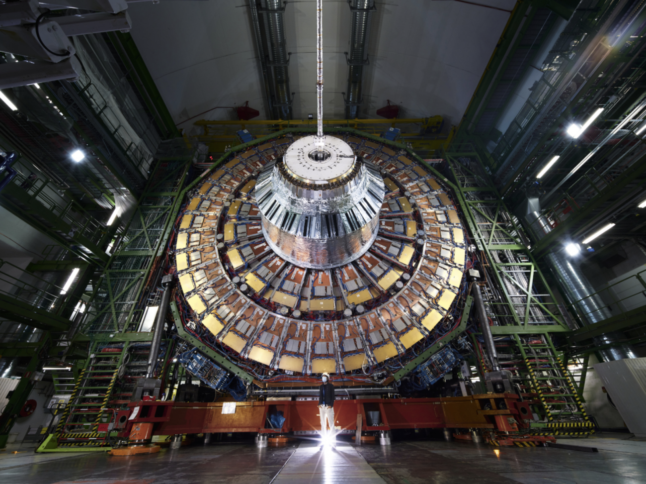
The upcoming upgrade of the LHC to the HL-LHC will pose significant challenges to the detectors due to the enhanced radiation levels and the increase in the number of pile-up interactions. To meet the increased demands, CMS has undertaken an extensive R&D program to upgrade many parts of the detector. This includes the replacement of the current endcap calorimeters with a high-granularity calorimeter (HGCAL), a sampling calorimeter consisting of 47 layers and almost 6 million readout channels. Silicon sensors have been chosen as one of the active materials for their excellent radiation hardness and fast signal formation. In total 620 m2 of silicon (about 26000 sensors) will be used in the entire electromagnetic section and high-radiation regions of the hadronic section, facing fluences of up to 1016 neq/cm2.
As sensors, hexagonal multi-pad planar silicon sensors cut from 8” (~20 cm) p-type wafers were selected, with two granularities: low-density (LD) and high-density (HD). The LD sensors have about 200 pads of ~1 cm2 and are produced from thinned float-zone silicon wafers of 200 m and 300 m thickness, while the HD sensors feature about 450 pads of ~0.5 cm2 and are produced by epitaxial growth on a handling wafer with 120 m active thickness. The thickness and granularity are adapted to the radiation field expected in the different detector regions. A majority of the sensors are full hexagons, but to produce an almost-circular fiducial coverage, partial hexagons of different shapes are also required. Pictures of an LD, an HD and an example LD partial sensor are presented in Figure 1.
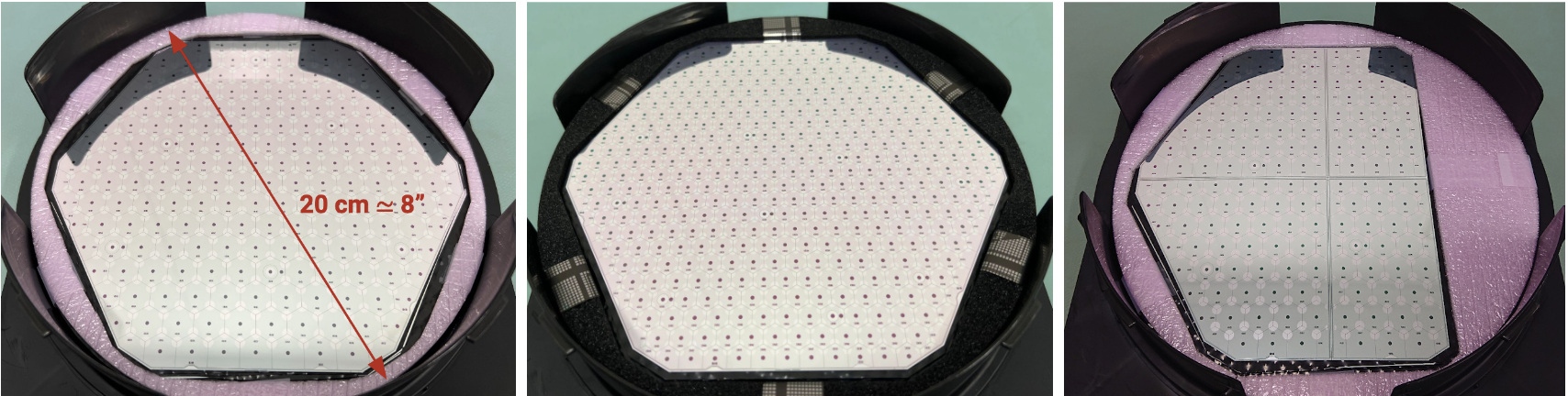
Figure 1: Low density full (left), high density full (middle) and example low-density partial (right) 8” silicon sensors.
Irradiation campaign
To establish the bulk radiation hardness of the full silicon sensors, a neutron irradiation campaign was needed covering a fluence range from 1014 - 1016 neq/cm2. Due to the sensors’ large size, bulk radiation damage studies were initially limited to smaller single-diode test structures taken from the same wafers as the hexagonal sensors, until the CMS collaboration developed the required infrastructure and procedures for the irradiation and subsequent electrical characterisation [1].
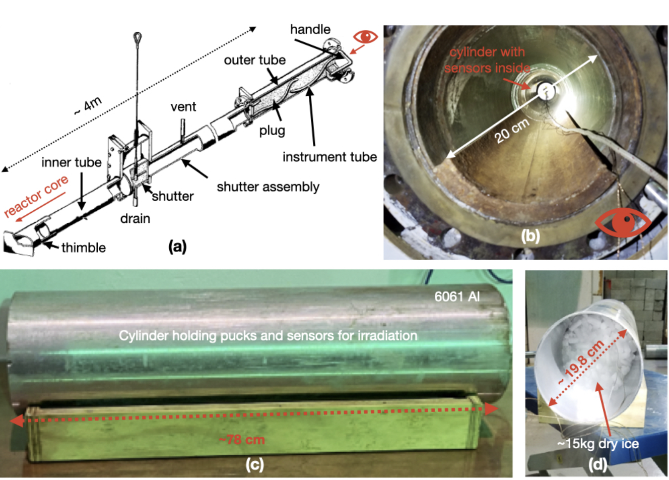
Figure 2: Schematic of the beam port sample delivery system at RINSC (a), view into the beam port (b), sample delivery cylinder containing the sensor-holding hockey pucks (c) and the dry ice used for cooling the sensor during irradiation (d) [1].
The irradiation facility established in this endeavor and able to expose such large objects to ~1016 neq/cm2 was found to be the Rhode Island Nuclear Science Center (RINSC), US. In RINSC, a 2MW light-water cooled, pool-type reactor, samples are irradiated in the reactor beam port with a diameter of 20 cm, as shown in Figure 2. Up to four sensors are stacked inside so-called hockey pucks (Figure 3) and inserted into the beam port in a cylinder alongside dry ice for cooling during the irradiation.
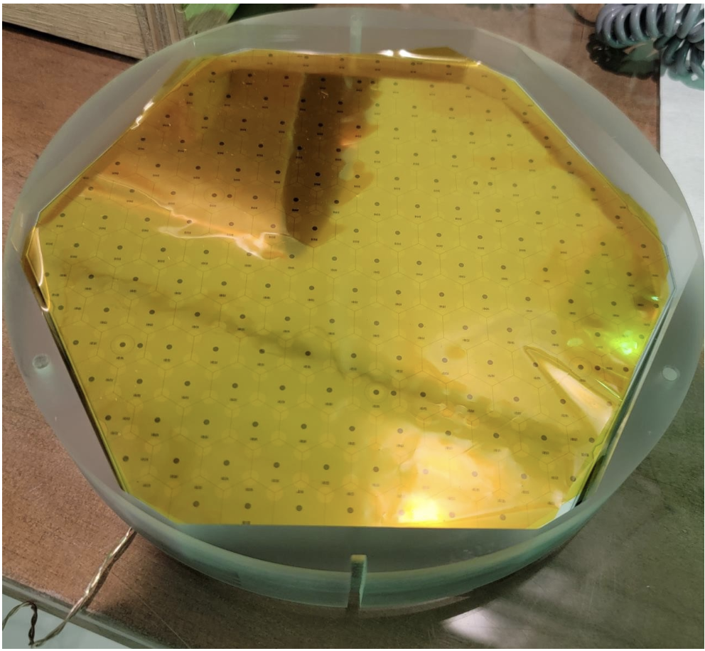
Figure 3: Full size LD sensor inside an acrylic hockey puck covered with Kapton foil. Apart from the shown acrylic puck, different puck materials were tested, including wood, PEEK and aluminum.
During irradiations, the reactor is operated at almost constant power, delivering a fluence of 1015 neq/cm2 in about 20 min. To further monitor the delivered fluence, reference silicon diodes as well as ultrapure iron foils are irradiated together with the HGCAL silicon sensors. The extraction of the depletion voltage and the dark current of the diodes as well as gamma spectroscopy measurements of the iron foils allow for a good assessment of the integrated fluence over the full fluence range under study.
Since August 2020 until today, 25 irradiation campaigns have been performed, including prototype sensors from different production-process variants (e.g. thickness and granularity, p-stop layout and concentration used for inter-cell isolation, oxide process) and covering 10 fluence points.
Electrical characterisation
The full sensor measurements after neutron irradiation were performed in two similar probe stations at CERN and Texas Tech. University, as presented in Figure 4. The irradiated sensor is placed on a metal chuck for backside-biasing and cooled down to temperatures below -20°C to suppress the irradiation-induced dark current rates to a level not harmful for the testing infrastructure. The individual pads are contacted with spring-loaded pins of a probe- and switchcard ARRAY system [2]. For each sensor, the per-pad leakage current, the total current and the per-pad capacitance are measured as a function of bias voltage up to a maximum of 850 V before and after additional annealing steps of up to 80 min at 60°C. For the annealing steps the equivalent annealing time at 60°C calculated from monitoring the temperature during irradiation is taken into account.
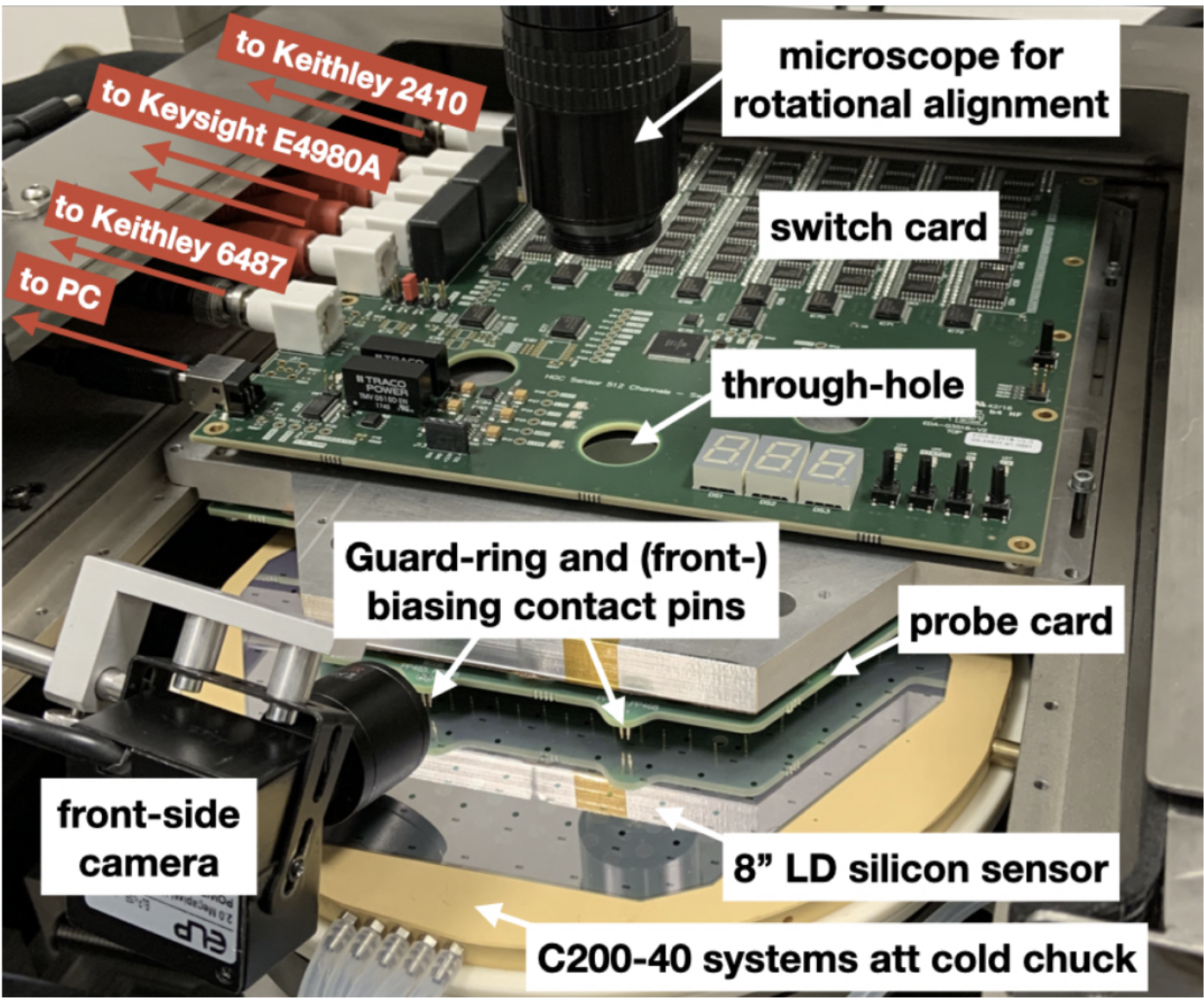
Figure 4: Low density sensor in a probe station before connecting it to the switch- and probecard system for per-pad leakage current and capacitance measurements at CERN.
Results
Figure 5 shows the measured per-pad leakage current at an effective bias voltage of 600 V (left) along with the depletion voltages of each pad extracted from per-pad CV measurements (right) for an example LD sensor irradiated to a fluence of 1.9 x 10¹⁵ neq/cm2 . The current scales with the cell size as expected; however, the current densities at a fixed voltage vary by roughly 20% throughout the sensor. Such profiles are visible in all sensors for both the current and the depletion voltage, both before and after annealing and consistent between sensors irradiated simultaneously. The pattern of the profiles slightly changed between different irradiation rounds. The observation is consistent with the presence of a fluence profile within the beam port.
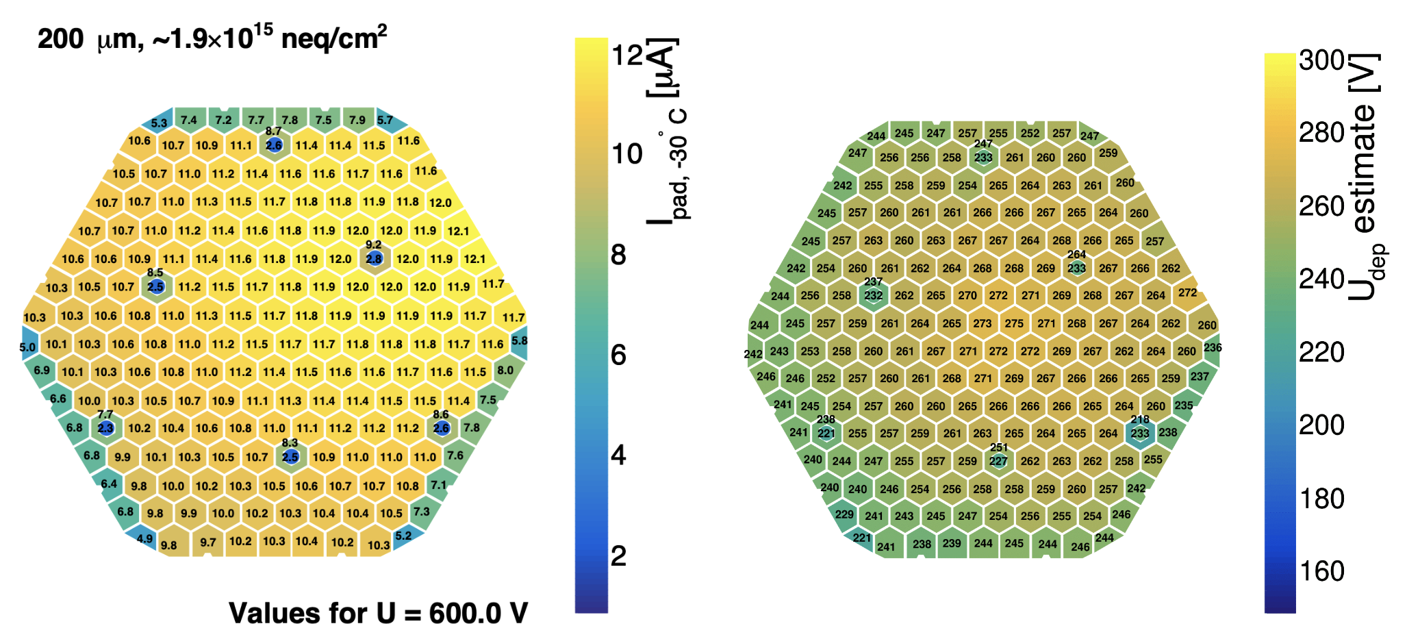
Figure 5: Per-pad leakage current interpolated to an effective bias voltage of 600 V (left) and the estimated depletion voltage extracted from CV measurements (right) for a low density sensor irradiated to a fluence of 1.9 x 10¹⁵ neq/cm2 before annealing. Before irradiation, the per-pad leakage current at room temperature was in the nA range and the depletion voltage was ~120V.
Furthermore, the measured current density scales with the fluence as expected, as shown in Figure 6. In early irradiation rounds [1], up to 40% difference was observed between target fluence and the fluence derived from the current-related damage rate, both for full sensors and reference test diodes. This could be improved through this study and the comparison with identical test diodes irradiated at the TRIGA reactor in Ljubljana, a well-established irradiation facility [3].
The numerical result for the damage rate obtained from these diodes is αVdep (-20°C) = (6.8 ± 0.1 [non-correlated] ± 0.7 [correlated]) x 10-19 A/cm, well in agreement with the numerical result α600V(-20°C) = (7.2 ± 0.2 [Fluence, ann.] ± 0.4 [Chuck temp. var.] ) x 10-19 A/cm from irradiations at RINSC using 8” sensors. The damage rate is independent of the different material properties or sensor designs, as visible in Figure 6 for different sensor types at a bias voltage of 600 V extrapolated to a temperature of -20°C.
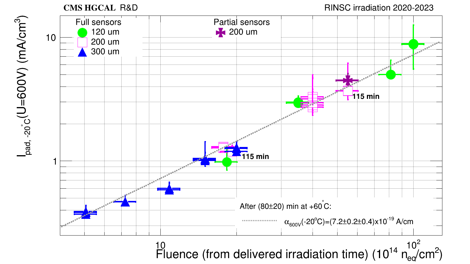
Figure 6: Volume-normalized per-pad leakage current interpolated to an effective bias voltage of 600 V as a function of irradiation fluence. All sensors are annealed 80 min at 60°C if not stated otherwise. Besides the sensor thickness and granularity, data of twelve different production process variants are included, showing consistent behavior in the damage rate.
Conclusion and outlook
The experimental verification of the radiation hardness is an essential part of the prototyping of the CMS HGCAL. With the available infrastructure at RINSC, for the first time full 8” sized silicon sensors were irradiated with neutrons and tested for the electrical properties (IV, CV) afterwards. Within this study the RINSC fluence assessment was validated and cross checked. A non-uniform flux profile across the sensor area was observed with variations within ~20%. The high-voltage stability of the sensors up to fluences of 1x10¹⁶ neq/cm2 was confirmed through the electrical characterisation as presented above.
In parallel, charge collection measurements are ongoing on single diodes and full sensors to ensure that the signal loss after neutron irradiation stays within acceptable limits. Furthermore, the effect of X-ray irradiation on the oxide layer of the HGCAL sensors were studied in test structures from HGCAL wafers [4]. This led to a selection of an oxide production process compatible with the well established 6” process used for instance in the CMS outer tracker.
Based on the results already collected, the HGCAL silicon sensors are expected to survive the entire duration of the HL-LHC operating period.
References
[1] CMS HGCAL Collaboration, Neutron Irradiation and Electrical Characterisation of the First 8” Silicon Pad Sensor Prototypes for the CMS Calorimeter Endcap Upgrade, arXiv:2209.10159, accepted for publication in JINST, 2022
[2] E. Brondolin et al., ARRAY: An open source, modular and probe-card based system with integrated switching matrix for characterisation of large area silicon pad sensors. NIM A, 940:168–173, 2019, https://doi.org/10.1016/j.nima.2019.06.007
[3] TRIGA Mark II Research Reactor, Jozef Stefan Institute, Ljubljana, Slovenia, See http://www.rcp.ijs.si/en/
[4] M. M. Defranchis et al., Characterisation of the silicon oxide quality in HGCAL sensor prototypes, https://indico.cern.ch/event/1096847/contributions/4743792/