![]()
Towards radiation tolerant silicon sensors – News from RD50
The RD50 collaboration “Radiation hard semiconductor devices for high luminosity colliders” is working on the development of radiation tolerant silicon sensors for the detectors of the HL-LHC (High Luminosity-LHC) experiments. An introduction to the RD50 collaboration which comprises 49 institutes with 270 members and its wide range of R&D activities were given in a recent newsletter article [link]. Since then six months and two exiting RD50 Workshops have passed: The 22nd Workshop took place in Albuquerque at the University of New Mexico, USA in June 2013 [link] and the 23rd RD50 Workshop at CERN in November 2013 [link]. Both workshops counted more than 40 oral presentations and several moderated discussion sessions in which the different R&D programs were reviewed and new projects were shaped. Significant progress has been achieved in several of the RD50 research activities. In this newsletter two highlight topics are presented: (1) The development of thin p-type planar pixel sensors and (2) the identification of microscopic defects in the crystal bulk of the sensors that are the root to all radiation damage. For further topics, like exiting new results on sensors with intrinsic gain (low gain avalanche detectors) or the progress in device simulations of irradiated sensors, the reader is referred to the RD50 website.
1.A new option for HL-LHC pixel sensors: P-type silicon sensors.
Pixel sensor and module concepts are presently being developed in view of the tracking detectors upgrades of the HL-LHC experiments. These devices will have to cope with extremely high particle rates (high occupancy) and extreme radiation levels reaching up to 1 MeV neutron equivalent fluences of 2 x 1016 cm-2 and ionising doses of more than a gigarad. Furthermore, the requirements for high rate, highly efficient and high resolution tracking can only be achieved by covering bigger radii with high granularity radiation tolerant sensors (pixel detectors) with low material budget. Finally, and despite all the improved properties, detectors have to become more cost-effective to make the overall upgrade project financeable. In this context, RD50 is studying in close collaboration with the ATLAS Planar Pixel Sensor (PPS) group the potential of p-type silicon as sensor material. Contrary to the presently used n-in-n pixel sensor technology (n-in-n: n-type implants form the segmented front electrodes in n-type silicon) the n-in-p sensor technology offers several advantages. The production process is much easier (and less expensive) since a double-sided processing is not needed. Furthermore, the homogeneous backside of the n-in-p sensors is less problematic to handle, allows easier mounting of the sensors and enables easier wafer thinning methods. The latter are used to reduce the mass of the sensor and therefore the multiple scattering of particle in the inner tracking volume. The only potential drawback of this technology is the fact that spark protection has to be assured between the low potential of the readout chip and the edges of the sensor. However, feasible solutions have been developed and demonstrated to offer good protection up to more than 1000V.
Prototypes of p-type pixel sensors have been produced, irradiated and successfully tested. As for n-in-n pixel sensors, it has been shown that even after the highest expected HL-LHC radiation levels, enough charge is collected at the sensor electrode to produce a signal to noise ratio that allows for efficient particle tracking provided a sufficiently high voltage is applied. Figure 1 gives an example of signal measurements as function of applied voltage. The dotted red line indicates the threshold for detection in this specific test run. P-type sensors are thus well suited to become a cost-effective sensor option for future radiation tolerant pixel detectors.
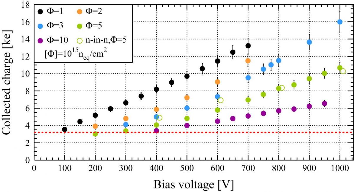
Figure 1: Collected Charge (MPV – Most Probable Value) for neutron irradiated n-in-p planar pixel sensors of 285 micrometer thickness. The measurements were performed with a beta-source (90Sr) as function of the applied bias voltage. The dotted red line indicates the tuned threshold of the sensors, 3200 electrons [taken from D.Forshaw, NIMA 730 (2013)44-49].
A question under study is the optimal thickness of the sensors, which impacts on the one hand on the material budget, but on the other hand also on the collected charge (signal) of the sensor. Surprisingly, recent measurements have shown that after high levels of radiation thin detectors can deliver even higher signals than thick sensors. This is demonstrated in Figure 2 for n-in-p-type pixel sensors with different thickness. It can be seen that for sensors exposed to 2 x 10¹⁵ neq/cm2 the optimal thickness is 150 micrometer if 200-300 V are applied to the sensor.
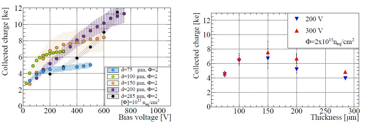
Figure 2: Comparison of collected charge as measured with a Sr90 source on irradiated p-type pixel sensors with different thickness bump-bonded to ATLAS FEI4 readout chips. [Figure taken from: S.Terzo, 23rd RD50 Workshop, CERN, Nov.2013].
This striking result is originating from the fact that charge collection after extreme particle fluences is impacted by very strong charge trapping (charge loss) which reduces the advantage of thick sensors. Furthermore, thin sensors profit from the higher electric field strength at same voltage.
Conclusion on the p-type pixel sensors
For the outer tracking detectors (strip sensors) n-in-p silicon sensors have become the baseline solution for the HL-LHC Trackers of ATLAS and CMS. For the pixel sensors n-in-p sensors are on their way to become a very reasonable solution for at least the outer pixel detector layers in the HL-LHC.
2.Microscopic defects – The root of all radiation damage
The radiation induced degradation of silicon sensor properties is caused by radiation induced electrically active microscopic defects within the crystalline bulk of the sensor. Within RD50 these defects are characterized and identified with various defect spectroscopy techniques. The aim is to get a deeper understanding of the mechanisms that degrade the performance, deliver reliable input for TCAD device simulations and eventually develop strategies how to mitigate radiation damage by defect engineering or other methods.
There is no lack of defects within the semiconductor bandgap of irradiated silicon. The task is therefore to identify those defects that are contributing to the performance degradation and determine all their characteristic properties. These properties include their concentration, location in the band gap, capture cross sections for electrons and holes and their stability over time and finally the question if they are of donor or acceptor type. While donors can be positively charged or neutral, acceptors can be negatively charged or neutral. The balance between positively charged and negatively charged defects will finally determine which sign and net concentration the space charge in the sensor has and consequently how much voltage has to be applied to fully deplete a silicon sensor of free charge carriers. RD50 has made enormous progress on the identification of those defects. Within a dedicated RD50 Working Group called WODEAN a large set of irradiated silicon sensor samples was produced and analysed in an co-ordinated effort by several institutes employing different defect characterization techniques. Figure 3 gives an overview about defects that have been identified to play a major role for the radiation damage of silicon sensors. The lines indicate the positions of the defect levels in the silicon semiconductor bandgap. Donors are marked in green while acceptors are marked in red. The textboxes give an indication for the impact of the defect level on the detector performance.
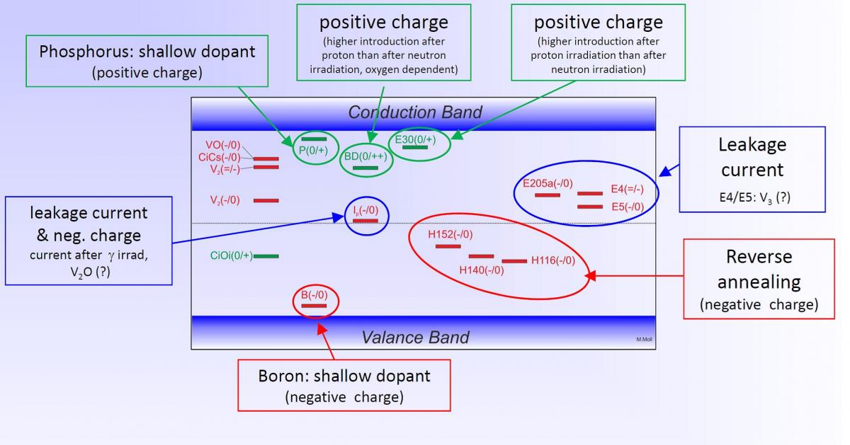
Figure 3: Defect levels in irradiated silicon which major impact on the tracking detector performance [Figure taken from: M.Moll, Vertex 2013].
One example for a link between microscopic measurements and macroscopic observations shall be given in the following: Figure 4 (top) shows a very remarkable result. If oxygen rich epitaxial n-type silicon is irradiated with 23 GeV protons the space charge remains positive (“no space charge inversion”). If the same material is irradiated with neutrons the space charge becomes more negative with increasing neutron fluence and eventually changes the sign of the space charge to negative (“SCSI - space charge sign inversion”). This so-called “Neutron-Proton-Puzzle” can now be explained by the fact that proton damage produces more point like defects with respect to cluster related defects than neutron irradiation. This is shown in Figure 4 (bottom) which was obtained with the TSC – Thermally Stimulated Current method. Each peak in the spectrum corresponds to a defect level in the bandgap. The defect E(30K) which introduces positive space charge is much more pronounced after proton irradiation than after neutron irradiation. The defects H(116K), H(140K), H(151K) which are providing negative space charge are however produced in equal quantities after both types of irradiation.
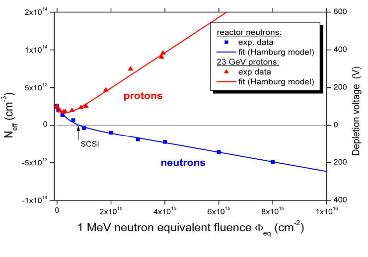
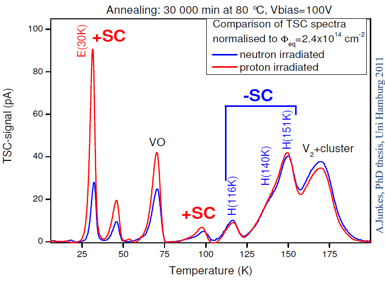
Figure 4 (top) Evolution of effective space charge in epitaxial silicon detectors after exposure to 23 GeV protons or reactor neutrons. (bottom) Thermally Stimulated Current (TSC) measurements on the same type of sensors [Taken from PhD thesis of A.Junkes, University of Hamburg, 2011].
Conclusion on defect investigations
The defect levels responsible for the introduction of negative and positive space charge after irradiation of silicon devices with hadrons or gamma rays have been identified and characterized including the defects that cause the so-called reverse annealing. The defects delivering the main contribution to the leakage current have as well been identified. The open question remains which are the defects that contribute most to the charge trapping (charge loss) in silicon devices after irradiation.
Summary
Recent progress of the RD50 collaboration in understanding the microscopic defects that cause the radiation induced degradation of silicon sensors in the LHC experiments as well as on the development of p-type silicon pixel detectors has been reported as part of the RD50 work program.
More information:
RD50 website: http://www.cern.ch/rd50
RD50 Co-spokespersons: Gianluigi Casse and Michael Moll
Further reading (p-type planar pixel sensors)
- D.Forshaw, Recent results of the ATLAS upgrade Planar Pixel Sensors R&D project, NIMA 730(2013)44-49.
Further reading (Radiation induced defects)
- R.Radu et al., Radiation damage in n-type silicon after electron irradiation with energies between 1.5 MeV - 15 MeV, NIMA 730(2013)84-90.
- A.Junkes, Status of defect investigations, PoS(Vertex 2011)035.
- I.Pintilie et al., Radiation induced point- and cluster-related defects with strong impact on damage properties of silicon detectors, NIMA 611 (2009) 52-68.
====
The links indicated within the article:
Newsletter: http://ep-news.web.cern.ch/content/rd50-radiation-tolerant-silicon-detectors-1
22nd RD50: https://indico.cern.ch/conferenceDisplay.py?confid=209612
23rd RD50: https://indico.cern.ch/conferenceDisplay.py?confId=265941