![]()
RD53: Development of pixel readout integrated circuits for extreme rate and radiation.
In June 2013 the LHCC has endorsed the establishment of a new R&D collaboration, RD53, to address the challenges of making readout integrated circuits for the phase 2 pixel detector upgrades of ATLAS and CMS, as well as long term developments of interest to CLIC. A combined effort between ATLAS, CMS and LCD was proposed as the most efficient manner to resolve the common challenges ahead. This new collaboration of 17 institutes and ~100 members will over the next years develop the methods and design foundation needed to produce pixel integrated circuits that can deliver the higher performance required under the extreme conditions anticipated.
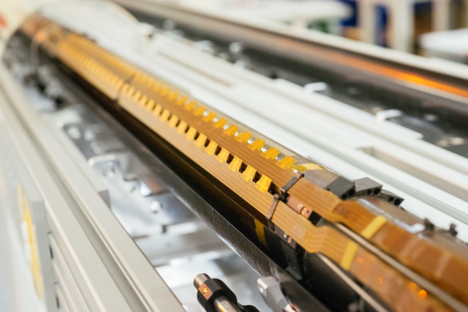
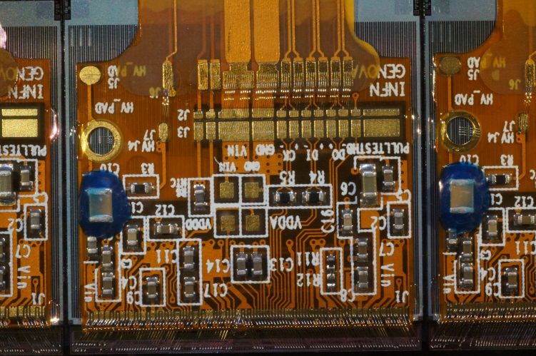
Figure 1: ATLAS IBL pixel staves (top) and ATLAS IBL pixel module (down).
Higher resolution tracking with pixel detectors will be vital to reconstruct events at the high collision rates at the HL-LHC with the very high track densities expected. The successful use of hybrid pixel detectors in the current LHC experiments has been a major achievement enabling a rich and successful physics program. Next generation pixel detectors will pose new challenges that require major advances in many aspects of pixel detectors, starting with their highly integrated readout electronics. The use of modern IC technologies is the only means to comply with the challenges of 4-8 times higher granularity, ~10 times higher hit rates and ~100 times higher readout data rates.
Figure 2: CMS phase 1 upgrade pixel module.
A 65nm CMOS technology node has been identified as a promising technology for the implementation of HL-LHC pixel chips with up ~500M transistors. This is a well-established IC technology that can be accessed relatively “affordably” in the initial R&D phase for small prototyping via MPWs (Multi Project Wafer), before large scale pixel chips are submitted for final prototyping and production. This technology node is also supported by the CERN microelectronics group (PH-ESE/ME) with a recently defined foundry frame contract and a design kit developed as a collaboration between CERN, Cadence (CAE tool supplier), IMEC (Europractice) and a commercial foundry. This technology has already been seen to have excellent radiation tolerance up to ~1MGy, while RD53 is already busy with extended radiation hardness testing/qualification to assess its radiation tolerance up to the required 10MGy level for the pixel detectors.
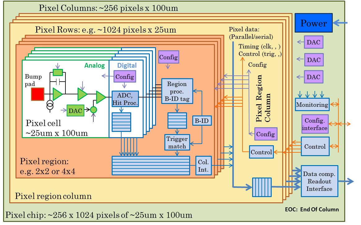
Figure 3: Phase 2 pixel chip architecture.
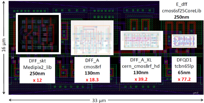
Figure 4: Relative size of rad hards Flip-flops in different technologies.
The first official meeting of the full RD53 collaboration will take place at CERN in April 2014 continuing the collaboration spirit established during a “pre-collaboration” workshop held at CERN in November 2012.
More information:
RD53 proposal: https://cds.cern.ch/record/1553467
RD53 presentation for the LHCC:
http://indico.cern.ch/event/252473/material/slides/1?contribId=27&sessionId=0