FastIC and FastICpix developments

Precise time tagging is a hot topic in High Energy Physics and in other fields. A number of detector technologies are available but there are few multi-channel front-end ASICs capable of providing time tagging in the region of 10ps. This article describes two developments that are going on within the microelectronics section of the Electronics Systems for the Experiments group (ESE-ME). Both the FastIC and the FastICpix developments are based on a collaboration between ESE-ME and the Institut de Ciències del Cosmos of the University of Barcelona (http://icc.ub.edu/).
The collaboration started in 2016 after the authors of this note co-organized a one-week summer school in Barcelona about solid-state semiconductor radiation detectors. That school, called the first Barcelona Techno Week, was attended by more than 60 students, mainly from Europe but also from the United States, Canada and even New Zealand. We had excellent lecturers including Erik Heijne (CERN), Paul O’Connor (BNL), Angelo Rivetti (INFN-Torino) or Angel Rodriguez and Ricardo Carmona from University of Sevilla, who covered radiation detectors from the basic principles to the state of the art, from interaction of radiation with matter to applications. That was the school we would have liked to have attended when we started in the field of design of electronics for radiation detectors.
After that organizational experience, the authors decided to start the FastIC project to design an Application Specific Integrated Circuit (ASIC), in 65nm CMOS technology, for the readout of fast timing detectors with an intrinsic gain of ~105-106 (examples of these detectors are Silicon PhotoMultipliers, Micro Channel Plates or Photomultiplier tubes). The first prototype was submitted to fabrication in May this year and includes a fully functional design with 8 single-ended channels. The FastIC chip is designed to replace the NINO, an ASIC implemented in 250nm CMOS, and to improve on its performance. The NINO ASIC [1] was designed in 2004 for the ALICE Time of Flight detector and, to the credit of its designers, it is still today a reference for the readout of fast detectors with low jitter. However, there are a few limitations: the energy measurement, based on the Time-over-Threshold method is non linear, its power consumption is large and it does not have build-in testing capabilities.
As NINO is widely used outside of CERN we were able to obtain financial support for the project from the KT fund. This funding allowed us to hire a PhD student, Jose Maria Fernandez-Tenllado, and to contribute financially to the submission of two Multi-Project Wafer (MPW) runs. As chance would have it, the authors met Jose Maria Fernandez-Tenllado at the first Barcelona Techno Week. Jose subsequently came to EPFL for his Masters Thesis. While in Lausanne, he visited our CERN labs at the time we had an opening for a PhD position to work in the FastIC design and to which he successfully applied.
There are many challenges when designing electronics for the readout of fast detectors. One of the challenges is related to the interconnection between the sensor and the readout ASIC. The jitter, that is the uncertainty in the time measurement, has the following expression:
σt = σn / (ds/dt)
Where σn is the noise of the system and ds/dt is the derivative of the signal (which can be a voltage or a current signal). The intrinsic inductance of the interconnection filters the high frequency components of the signal delivered by the sensor reducing the slope of the input current pulse entering into the front-end [2]. Since the jitter is inversely proportional to the slope of the signal, it is degraded by the effect of the inductance. The input capacitance of the sensor is another factor that limits the slope of the signal at the preamplifier input. A careful study has to be done in order to optimize the input impedance of the electronics to avoid ringing in the signals due to resonances of the input network and the study also has to address considerations related to the optimum bandwidth of the input front-end. Designing for a bandwidth above this optimum there is a penalty in the jitter because of an excess in noise and in power consumption [3]. The large range in the input capacitance of the detectors and the input dynamic range for detectors like SiPMs (from a few μA to mA) make the design of the input stage and the signal processing very challenging (e.g. the input capacitance for MCPs can be in the order of ~10pF whereas the input capacitance for SiPMs can be from ~100pF to ~1nF).
Another challenge consists in the limitations imposed by the choice of the technological node for manufacturing the ASIC. Trends in the microelectronics industry and the need for increased signal processing speed and performances oblige the radiation instrumentation community to continue to follow Moore’s Law in the development of front-end electronics. Moreover, the adoption of new technologies can add significant benefits and open new applications. Therefore, the new front-end has been designed in the most recent CMOS technology to which we have regular access (65nm CMOS). However, each new technology node requires a significant effort to understand how high performance analog designs can be implemented. The main challenges imposed by the very deep submicron technology have been, in particular, the reduced power supply voltage (1.2V) that results in a reduction of the dynamic range, the reduction in the intrinsic gain of the transistor and increased gate leakage currents with respect to previous technological nodes.
FastIC
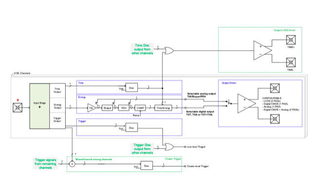
The FastIC chip reads out the signal delivered by the sensor and processes it in a current mode method. A block diagram is shown in Figure 1. The architecture is based on the HRflexToT chip [4].

Figure 1. Block diagram of the FastIC ASIC channel when programmed in a single ended architecture. The Input Stage, the Time, Energy and Trigger channels and the Output driver are shown.
The input stage generates three replicas of the incoming signal, the weight of each replica being different. The first replica, with the highest weight, corresponds to the timing signal that is sent to a fast current discriminator which compares the signal with a programmable threshold. This threshold can be set at level below the charge delivered from the sensor when a single photoelectron is detected. The leading edge of the signal at the comparator output retains the information of the time of arrival of the detected particle. The chip can be programmed to output this signal for each channel. It also outputs a fast-OR combining the timing signals of all the channels.
The second replica is processed by some circuitry in order to measure the deposited energy in the sensor. The processing chain contains a transimpedance amplifier, a shaper (with a selectable peaking time, the nominal being ~25ns-50ns), a peak detector and hold (PDH) and a discriminator that compares the output of the PDH with a ramp. The time duration of the digital pulse at the output of this discriminator is proportional to the charge delivered by the sensor.
The third replica is used for the trigger signal whose threshold is typically set to be higher than the threshold of the timing channel. Two trigger signals can be generated. The Low Level Trigger and the Cluster Level Trigger. The Low Level Trigger is the OR of the output of the comparators of the trigger channels and the Cluster Level Trigger compares the sum of the signals deposited in all the channels in a chip with a separate threshold. These trigger signals can be used to start the ramp generator for the energy to time conversion. Alternatively, the OR of the fast timing channels or a pulse fed externally into the chip can also be used for this purpose.
At the output of the time and energy processing branches, the channel can be programmed to provide (1) The Time-Of-Arrival information only, (2) the Time over Threshold information or (3) a combination of the two. In the first case, the energy branch is bypassed and as a consequence, the pulses at the fast discriminator output can be very short, the maximum flux that can be processed by the channel being only dependent on the signal of the detector itself. In the latter case, the channel generates two pulses for an incoming input signal. The first pulse’s rising edge contains the information of the ToA and the second pulse’s width contains the information on the linear energy measurement. The maximum count rate that the chip can process in this mode is ~2MHz.
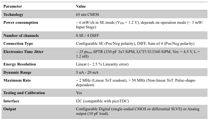
The input stage can be programmed to work in either positive or negative polarity. In the case of a detector with a differential output, the 8 single ended channels can be reconfigured into 4 differential channels. It is also possible to combine 4 channels and sum their signals at the ouput of the input stage. This active summation functionality is integrated to explore the impact of segmenting large SiPMs (with large capacitance) into smaller ones to achieve lower jitter while covering large detector areas. The expected performance of the chip is presented in Table 1.

In FastIC the readout channels are laid out in a linear way and the chip inputs are wire-bonded to a PCB or to a package. This interconnection scheme with its associated added inductance limits the time performance of the system as described above. Also, the large intrinsic capacitance in sensors like Silicon Photomultipliers leads to a reduction of the input signal amplitude in current sensing and processing circuits. The combination of both effects limits the slew rate of the signal and as a consequence the system suffers from an increased jitter. This lead the design team to propose a new sensor architecture whereby the sensor and readout electronics are intimately connected: the FastICpix concept.

