![]()
Wafer-level testing of CMS Outer Tracker ASICs
The Macro-Pixel ASIC (MPA) and Short-Strip ASIC (SSA) are the new read-out chips used to process particle hit signals of pixel and strip sensors in the upcoming CMS Outer Tracker of the High-Luminosity LHC Upgrade (HL-LHC). The two chips are produced by TSMCs 65nm fabrication process and were designed by the Outer Tracker ASICs Working Group of the EP-ESE-ME section. Together with the Concentrator IC (CIC), these ASICs will be deployed as the front-end read-out chain of the Pixel-Strip module (PS module) in the Outer Tracker. The read-out ASICs of the PS module have reached their final design iterations, code-named MPA2, SSA2.1 and CIC2.1. Throughout the last year, preparations have been on-going tirelessly for the large-scale production of the three chips. This includes the rigorous functional testing and electrical characterization of the silicon prototypes at the wafer-level stage.
The probing of the early-release engineering wafers provides a very large set of characterization data allowing to measure chip-to-chip variation and process variation, detect wafer pattern variations and gather all this testing data in an automatic and reproducible manner. This is an important and necessary step for the early detection of issues, assembly of test-modules, as well as preparation for large-scale production testing. The production testing of hundreds of wafers in face of their commissioning for the Outer Tracker Phase-2 Upgrade will be conducted by an external vendor upon selection by Invitation for Tender. Hence, the in-house testing experience of a smaller early batch of the ASICs is essential for the clear and comprehensive specification of the testing procedures towards the vendor.
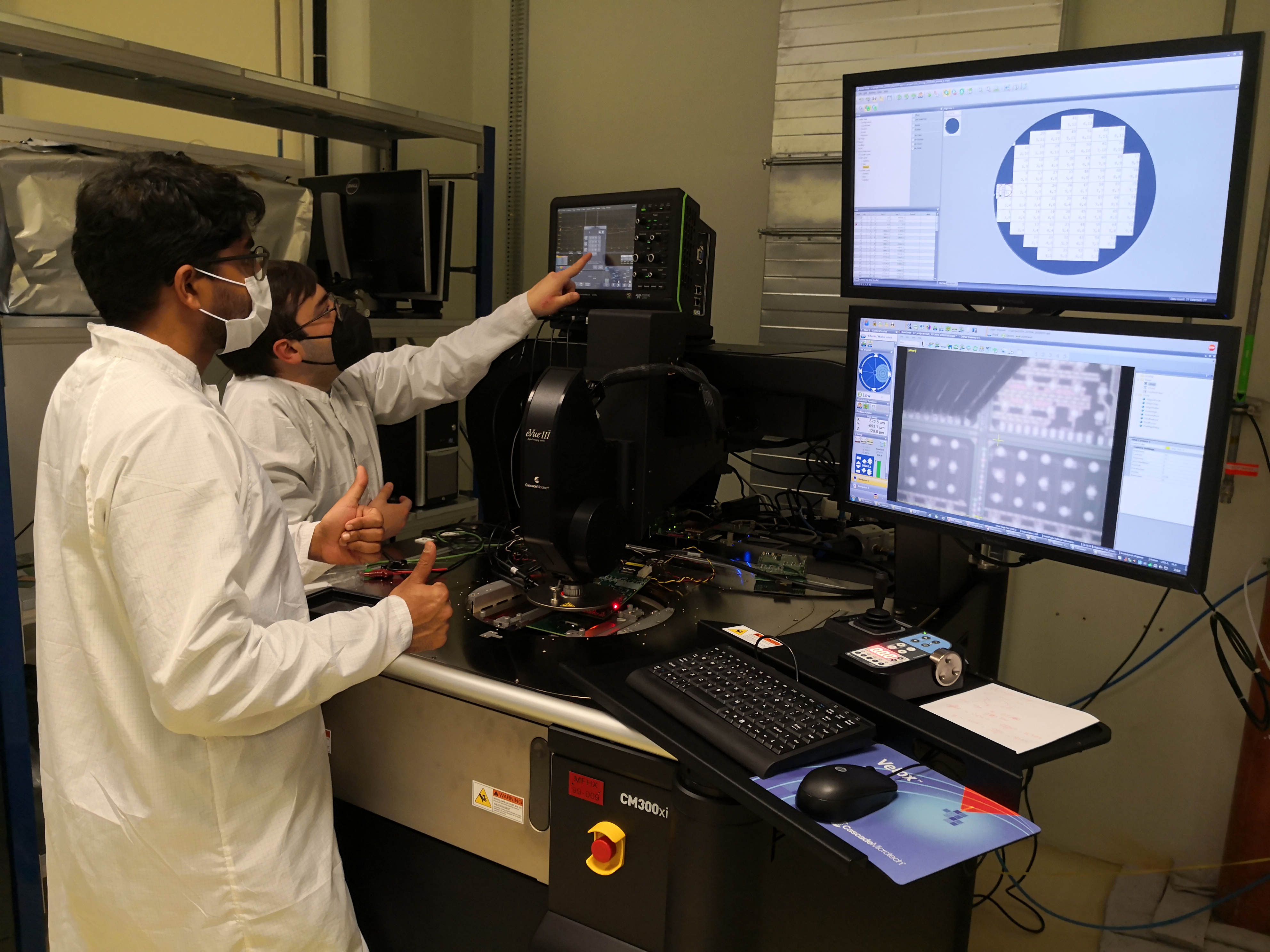
Figure 1. A class ISO 7 clean room facility provided by EP-DT, stands the Cascade Microtech 300mm wafer probing station.
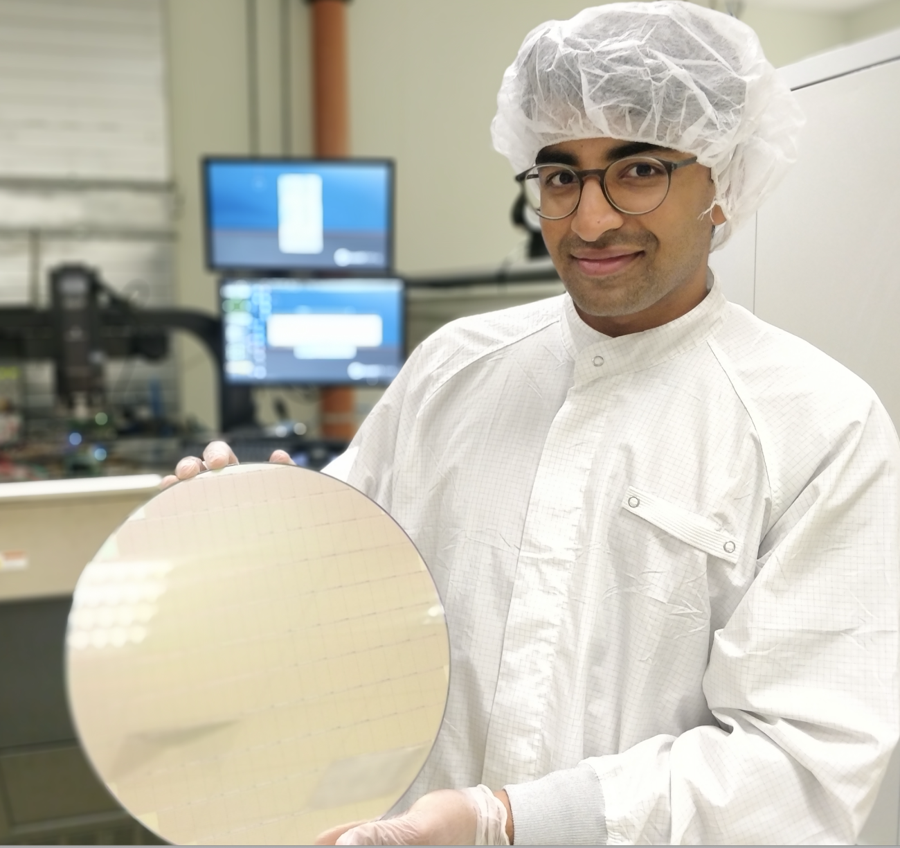
Located in the Department Silicon Facility (DSF), a class ISO 7 clean room facility provided by EP-DT, stands the Cascade Microtech 300mm wafer probing station (see Image 1). Over 18 MPA2 and 6 SSA2.1+CIC2.1 wafers have been tested using the probe station by the ASIC design team at EP-ESE-ME throughout the last year. Maintained by Jerome Alozy (CERN), the machine provides a powerful UI offering a suite of features regarding its ease-of-use and, most importantly, its remote interface for the automated probing of wafers. These features support the programming of complex wafer maps into the machine, allowing also the automated probing of multiple-project wafers (MPWs).
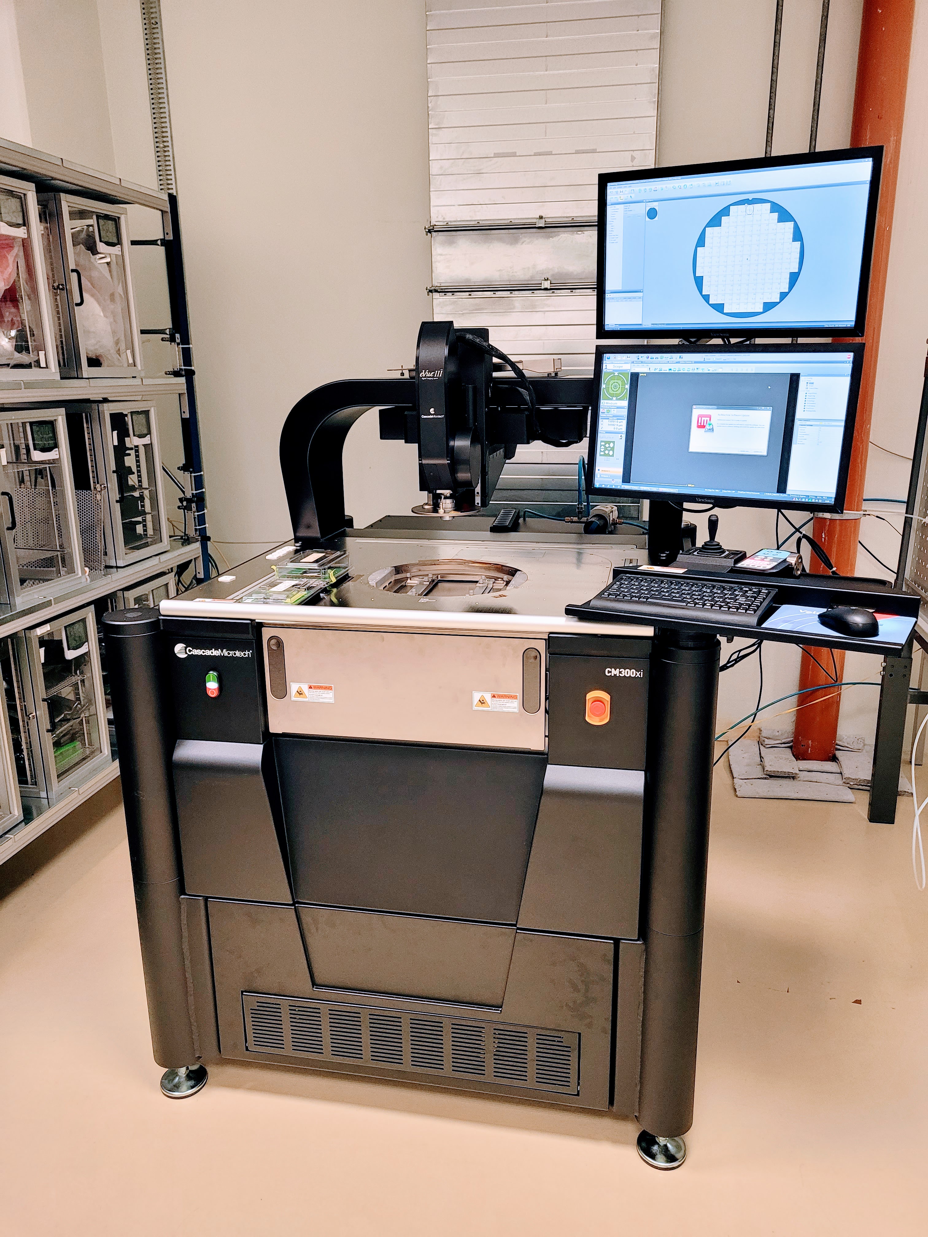
Figure 2. The measurement system.
After setting up the measurement system (see Image 2) and installing a custom designed probe card, a wafer is loaded into the machine by placing it on the wafer chuck. Next, the alignment of the wafer chuck needs to be completed. The rotation of the wafer chuck, the position of the scope and tilt of the probe tips can all be precisely adjusted to ensure a good contact between the probing tips of the probe card and the pads of a die (Image 3). Once the alignment has been completed and the probe station has been programmed with the wafer map, which includes the location, exact size and pitch of the dies processed on the wafer, the probe station is ready to be setup for automation.
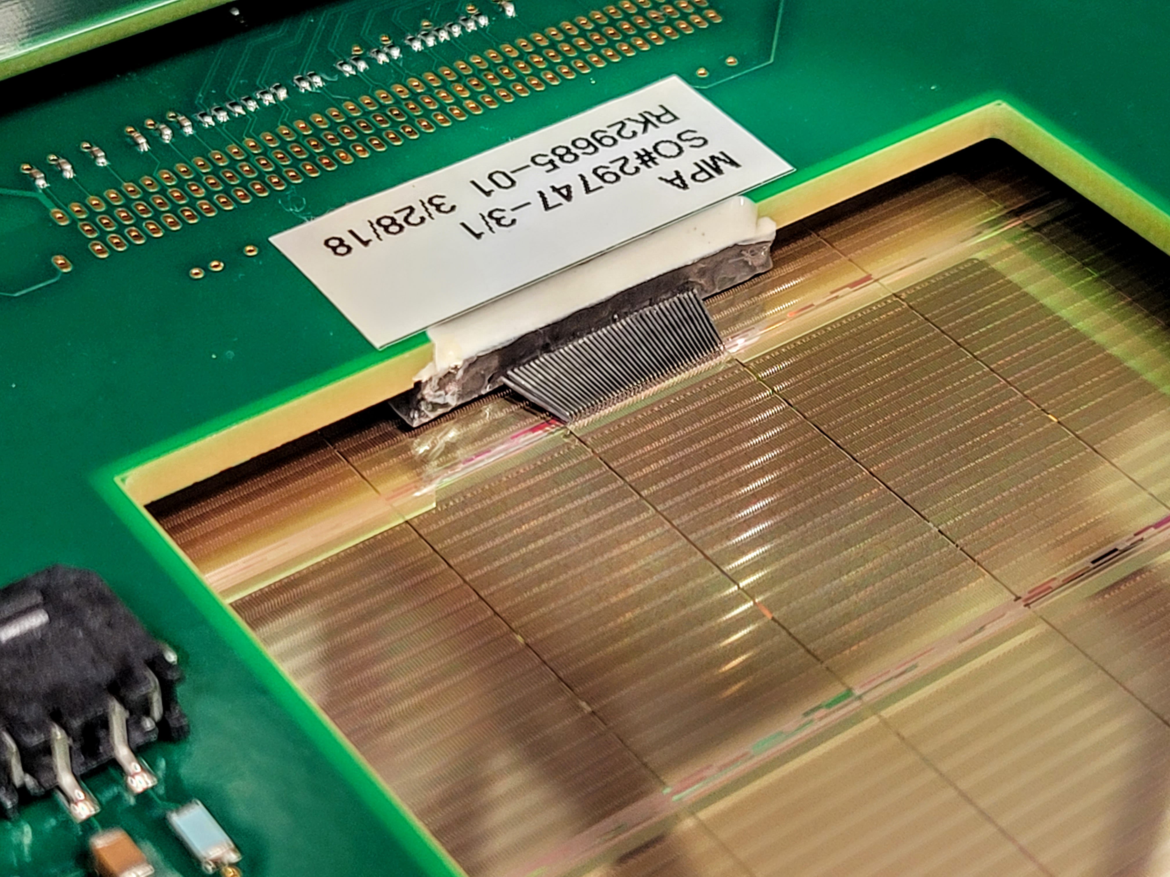
Figure 3. Detail of the chip showcasing the good contact between the probing tips of the probe card and the pads of a die.
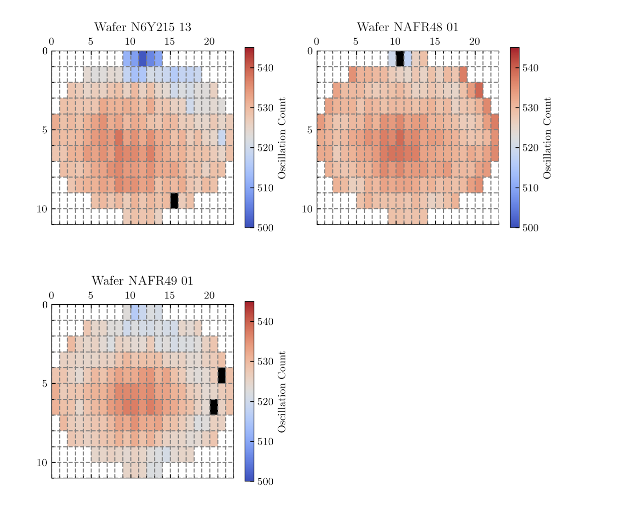
Figure 4. Example results, showing a “heat map” of a specific measurement made per chip and its variability across different wafers. Chips which fail a measurement are marked black.
With use of a NI GPIB interface the probe station can be controlled by string commands sent by a user on a connected PC. Remote interface commands include actions such as moving the chuck into contact or separation, stepping to adjacent dies, moving to specific dies, etc. In our testing system, we have made great use of python to script the remote control of the wafer probing machine, start the testing procedures per chip and also collect and analyze the results (Image 4). The probe station features an automated pattern recognition where the probe station software can be trained with a pattern unique to each chip. This allows to compensate for small drifts in the stepping lengths between dies and ensures an identical contact to each die during a probing procedure.
So far, 3550 MPA2 and 8988 SSA2.1 ASICs have been probed and have had their functionality verified with the probe station in DSF. Additional wafers to be probed are en-route to CERN. Chips that are asserted as good will be further processed to be used in PS-Module sub-assemblies for module testing campaigns, conducted by various CMS institutions such as Fermilab in the US and DESY in Germany. As such, wafer probing of silicon prototypes at EP-ESE continues to prove itself a vital aspect of the ASIC development activities and collaborations for CERN experiments.