![]()
ATLAS Tile Calorimeter Phase II Upgrade: entering production phase.
The start of the High Luminosity LHC is approaching at a fast pace. In order to be ready with its upgraded front-end electronics and data acquisition systems, ATLAS Tile Calorimeter (TileCal) community is now entering the production phase, after a long R&D period and many design reviews. The TileCal is a cylinder-shaped hadron sampling calorimeter with steel absorbers and scintillating tiles, oriented perpendicular to the beam axis. The light from the tiles is collected by wavelength shifting (WLS) fibers and then delivered to photomultipliers (PMT) to be later digitized by the front-end electronics, located at the outer radius of the calorimeter. The new trigger and data acquisition architecture and the harsh radiation environment requires a complete redesign and replacement of the on- and off-detector electronics. Now the digitized data will be sent to the off-detector electronics for every bunch-crossing of the LHC at 40 MHz rate.
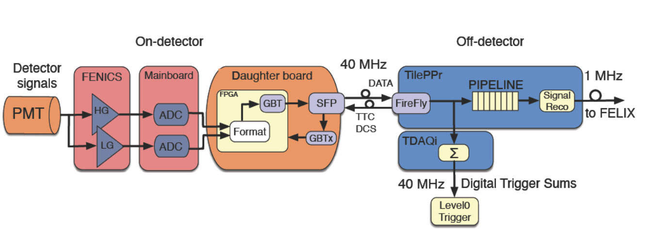
Figure 1. A simplified diagram of the upgraded ATLAS TileCal readout architecture.
Many sub-projects of ATLAS TileCal Phase II Upgrade already managed to finish the production and deliver the required items to CERN. The full quantity of “mini-drawers”, new support mechanics that are made from aluminum and provide housing and cooling for the Tile Calorimeter PMTs and front-electronics, have been produced at ITIM Cluj in Romania and at IFAE Barcelona in Spain. This design follows a new modular and redundant architecture of the front-end electronics. It will facilitate extraction and repair of the failures in a more restricted space during detector opening.
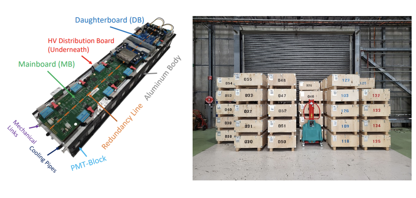
Figure 2. Fully assembled mini-drawer with PMTs and front-end electronics (left). A stack of delivered mini-drawer mechanics at CERN (right).
While we cannot upgrade the detector itself, including the scintillating tiles and WLS fibers, we will replace about 10% of the photomultipliers that suffered from the accumulated charge. A contract with PMT manufacturer has been signed, the production line is getting ready, and people in several labs are eagerly awaiting the flux of new PMTs, to measure their parameters and qualify them for use in the detector. Long-term tests showed that the latest version of the PMT is more robust with respect to the accumulated charge. In addition, all PMTs will receive new “active” high voltage dividers that are stable at high currents. More than 11000 dividers were produced in Cluj Romania, and almost all of them were tested and certified. The massive production of the very-front-end cards that shape and amplify the signal from the PMT, called FENICS, has also recently started, after the successful pre-production and testing campaigns. The 11000 boards will be produced and tested in the burn-in station at LPC Clermont-Ferrand in France to be ready in time for the assembly.
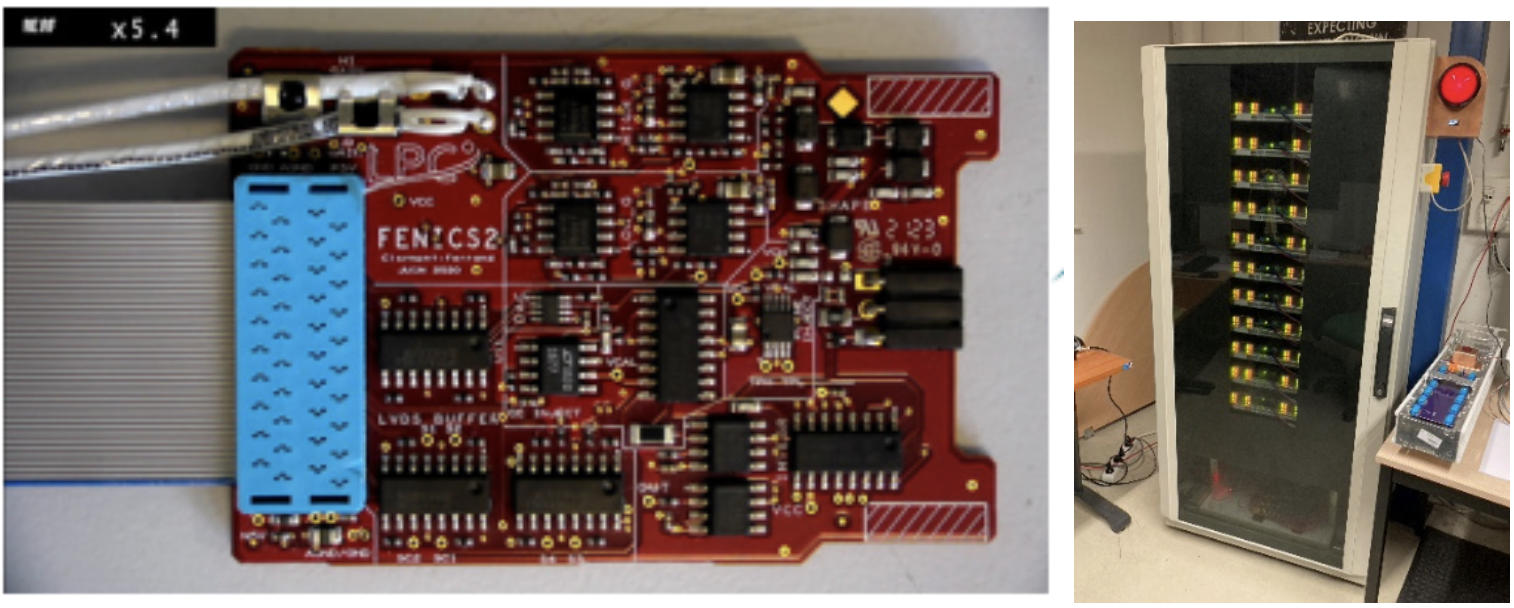
Figure 3. The very front-end FENICS card and its burn-in station at Clermont-Ferrand, France.
The signal from the front-end cards will be digitized by the ADCs located on the mainboard, a large card that collects the signal from FENICS and sends digitized data to the daughterboard for further shipment to the off-detector electronics. The mainboard design fosters the independence and redundancy principles to minimize the effects of malfunction due to power, connectivity or other issues. All PCBs have been produced and more than one half of the needed quantity have been assembled and tested. A significant number have already been delivered to CERN.
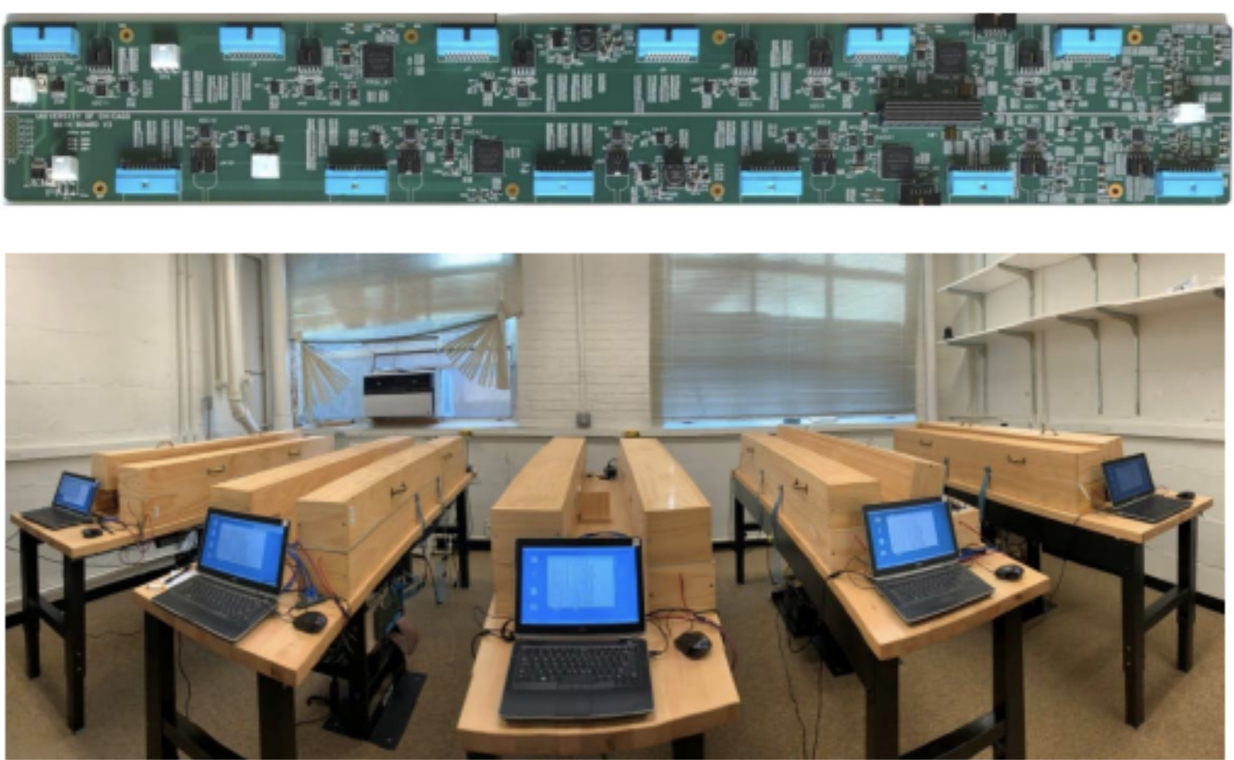
Figure 4. Mainboard hosting the ADCs and corresponding burn-in stations at Chicago, USA.
The data from the ADCs have to be shipped to the off-detector electronics via high-speed optical links, using GBT protocol developed at CERN. This task is performed by daughterboard with high-performance FPGAs, following the same redundancy scheme as the mainboard. Strict radiation tolerance requirements demanded several iterations of the design, and we even had to move back to the previous generation of Kintex UltraScale FPGA technology as the top-of-the-line process turned out to be less robust under the high flux of ionizing particles, exhibiting single event effects (SEE). The design of the latest version of the daughterboard is close to completion after the massive campaign of irradiation tests. The final design review is planned for this year (2023) to allow for timely production.
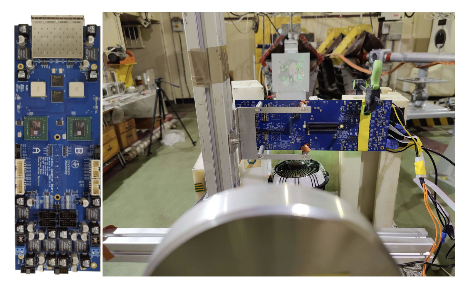
Figure 5. TileCal Daughterboard with Kintex UltraScale FPGAs and SFP+ optical modules.
The massive flux of data (40 Tbps) coming from the front-end electronics will be pre-processed for the trigger purposes and processed and formatted for the next stage of the data acquisition. This will be done by Tile PreProcessor (PPr) ATCA boards, which will host four compact processor modules (CPMs) to read and pre-process the data inside the Kintex UltraScale FPGAs in real time and the interface with the trigger and data acquisition system – TDAQi, a rear-transition module, with a plethora of high-speed optical links. These complex boards have up to 16 layers and are using latest materials and technologies for the high-speed data transmission and boasts large FPGAs and multiple optical interfaces.
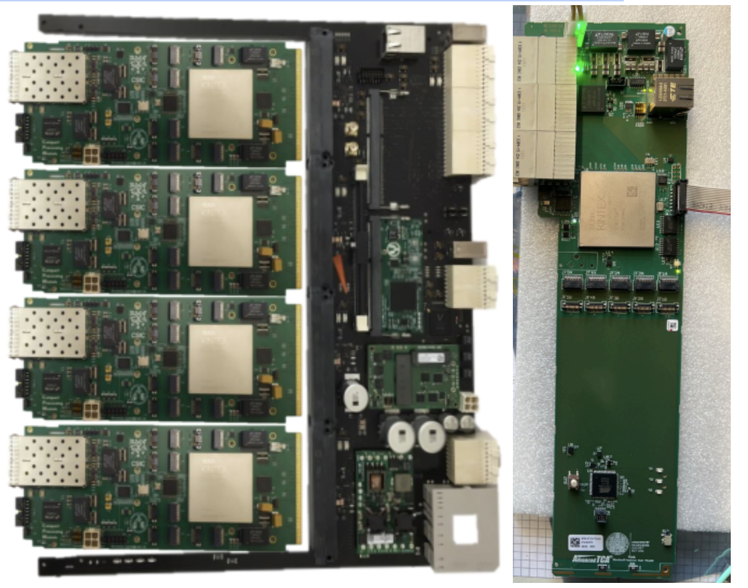
Figure 6. The preprocessor (PPr) ATCA blade and Trigger/DAQ interface (TDAQi) RTM.
The on-detector electronics requires power, both low (LV) and high voltage (HV). While the LV power-supplies are located on-detector to efficiently provide high current, the HV in the new design will be regulated in the control cavern, away from the hard radiation environment. Consequently, the LV power-supply components, namely the power-bricks, require stringent radiation testing to ensure stable working conditions during the whole HL-LHC data taking. In several cases, the design team had to test many chips from different manufacturers before selecting the one fulfilling all the requirements.
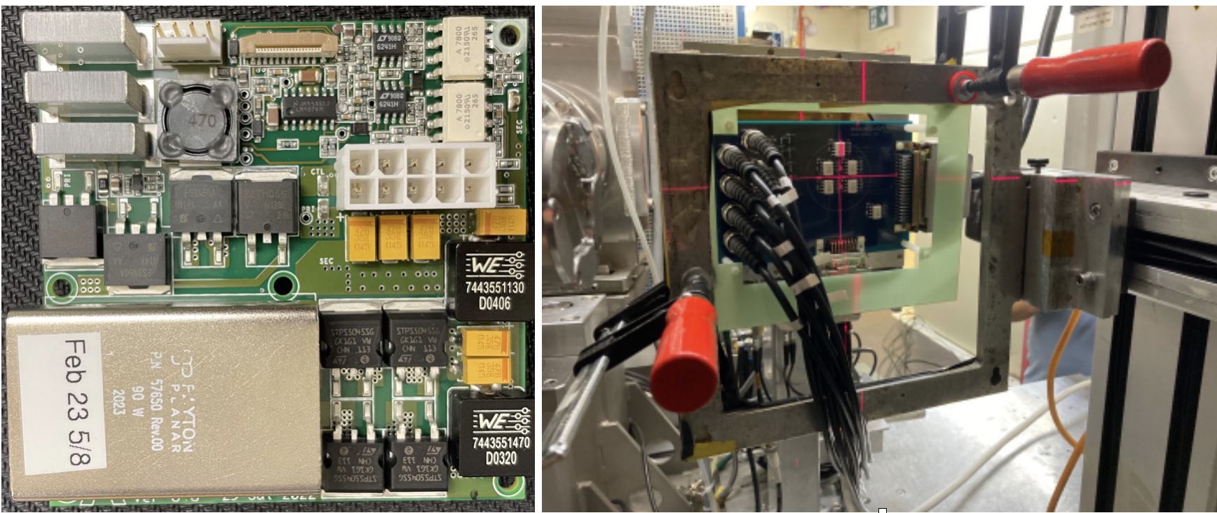
Figure 7. Low Voltage Power Supply (LVPS) brick and radiation test of optical isolation amplifiers.
Following the upgrade of the read-out electronics, calibration systems also have to evolve and fit the new architecture and radiation hardness requirements. The on-detector electronics of Cesium calibration system had to undergo a complete redesign, and now will profit from the lpGBT chip to communicate with the off-detector equipment. First prototypes were produced and tested, and the team is hoping to finalize the design soon to start the board production next year.
Similarly, the laser calibration system will be upgraded with new electronics, according to new DAQ architecture and will include necessary modifications to the laser box to inject through an optical sphere a steady light to simulate pile-up conditions for more precise calibration of the PMTs. A first prototype of the board is now being tested.
The electronics boards produced at different Institutes and delivered to CERN will have to be assembled and tested prior to the installation in the experimental cavern during LS3. These tasks necessitate specialized and efficient test stands and installation tools. The tools and stands were produced and are awaiting their delivery to CERN. As the power and cooling services might not be available during the installation, a self-contained and portable testing equipment is required, including LV and HV power supplies, to provide electronics testing facilities during the assembly and maintenance, a truly portable (with two handles for transport) test-box named “Prometeo” was designed, and latest prototype shows encouraging results.
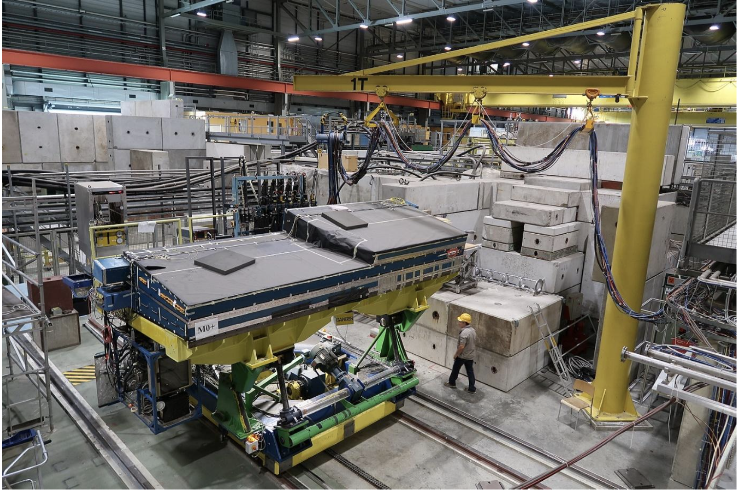
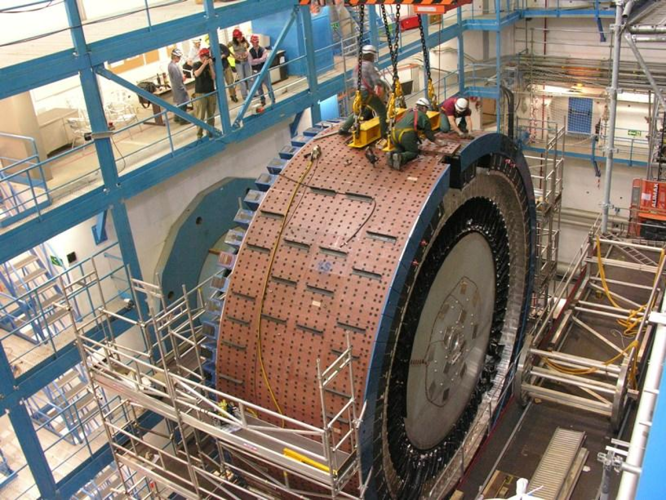
Figure 8. A bundle of ATLAS TileCal modules on the rotating table at the H8 test beam area at CERN.
As they used to say, everything works in the lab. Experience shows that it is absolutely necessary to test and integrate the boards together in the vertical slice tests (VST), and finally in the real environment and the detector, like the test beam setup. Getting real data with new electronics allows not only to test the new piece of equipment, but also to attract and train new experts, gain operational experience that is crucial for the long-term running of the experiment. TileCal usually organizes two test-beam sessions per year, and many young scientists get a chance to contribute to the success of the project and with first-hand experience. In addition, during LS2 we installed a “demonstrator” drawer inside one of the TileCal modules in ATLAS, which while implementing the upgraded clock distribution and readout architecture, is compatible with the existing trigger and data acquisition system. Recently it was updated with the latest design of the mainboards and daughterboards. It will provide a lot of operational experience and performance data ahead of the start of HL-LHC.
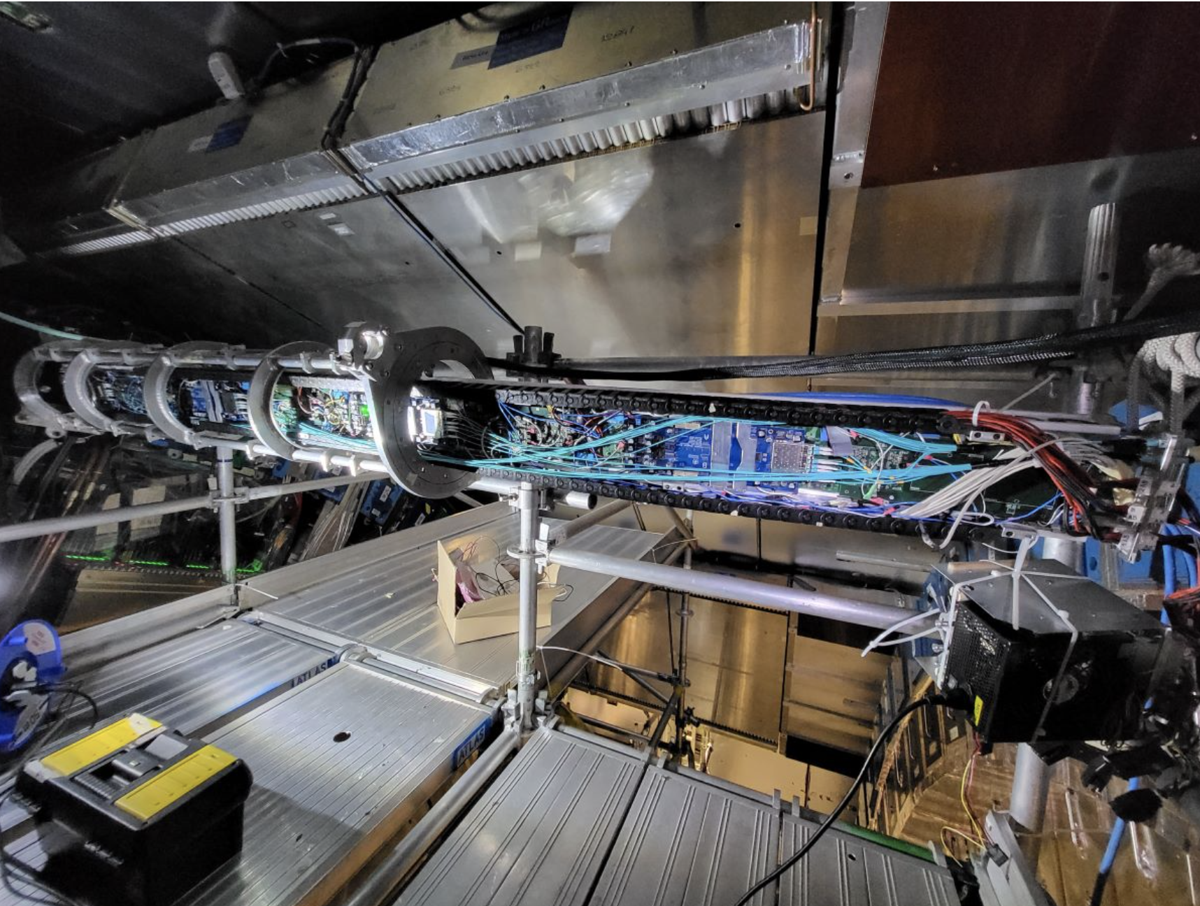
Figure 9. Insertion of the “demonstrator” electronics drawer into the ATLAS TileCal.
To summarize, the ATLAS Tile Calorimeter Phase II Upgrade project is now shifting its gears from design and prototyping into the production phase. Along the way we managed to solve many unexpected problems, dealt with shortages of electronics components, made difficult choices, and even had to revert to older technologies. As some components are now fully produced, we face an unusual challenge of properly storing the electronics boards so they are intact and ready for assembly in 3-4 years’ time. Still, it is always nice to be earlier than later!
Further reading
Upgrade of the ATLAS Hadronic Tile Calorimeter for the High Luminosity LHC - https://indico.tlabs.ac.za/event/113/contributions/2381/
Development of the PreProcessor Modules for the Upgrade of the ATLAS Tile Calorimeter Towards the High-Luminosity LHC - https://indico.cern.ch/event/1109460/contributions/4893232/
ATLAS Collaboration, Technical Design Report for the Phase-II Upgrade of the ATLAS Tile Calorimeter, CERN-LHCC-2017-019 - http://cds.cern.ch/record/2285583