![]()
Pushing the boundaries of monolithic CMOS sensor technologies

Silicon solid state detectors have been developed over a long time to address the challenges of particle tracking and vertexing. At the LHC, when the machine reaches its full design regime, it collides proton bunches at a rate of 40 million times per second. To capture these events and minimise the loss of information, physicists need very fast cameras able to deal with this rate. The high-luminosity LHC (HL-LHC) will place severe demands on the LHC experiments, currently working to develop even more powerful silicon detectors to accommodate a “pileup” level of 200 events per bunch crossing contrasted to the 60 events per bunch crossing achieved so far.
Developing new silicon sensors and readout chips remains vital for exploring new physics at the LHC. One of the most widespread technologies are the so-called hybrid pixel detectors, where the sensor and readout electronics chips form a “sandwich” filled with an array of microscopic solder balls, each one connecting a single detector pixel to its own unique readout pixel. This approach delivers optimal speed of parallel processing and good radiation hardness while being compatible with almost all commercial CMOS processes. Over the past years, thanks to the sustained efforts of many experts, an impressive collection of hybrid pixel tracking detectors has been brought to completion in many detector facilities. However, hybrid chips present certain challenges when used in particle detectors, namely the more complex and costly assembly procedure, higher analog power dissipation due to a larger sensor capacitance, and higher material budget in a tracking system.
To address these challenges, Monolithic Active Pixel Sensors (MAPS) are pursued as an alternative. Compared to hybrid pixel detectors, MAPS combines sensor and readout circuitry in a single silicon chip, thus avoiding some above-mentioned challenges. MAPS technology therefore can offer certain advantages in terms of detector assembly, production cost, material budget, and lower detector capacitance for lower analog power or a thinner detector layer, all important for large area detectors, while it can also offer high granularities. In that sense, MAPS offers a promising alternative, and efforts are ongoing to push the readiness of this technology for future detectors.
Pushing the boundaries of MAPS technology and paving the way to new applications represents one of the long-term goals of the EP department's R&D on monolithic sensors and lies at the core of WP1.2 activities. The WP focuses on the development of monolithic sensors in sub-100nm CMOS technologies. The TPSCo 65 nm ISC CMOS imaging technology has been selected as the first one to be investigated, in synergy with the development towards the Inner Tracking System 3 (ITS3) upgrade for the ALICE experiment. As part of the EP RnD programme, this effort within the WP1.2 of the EP RnD program and within the ALICE experiment builds on previous experience gained with the use of MAPS technology in high-energy physics. Monolithic pixel technology has previously been used for the STAR experiment at the Relativistic Heavy-Ion Collider at Brookhaven National Laboratory, while more recently it was adopted for the upgrade of the ALICE Inner Tracker, ITS2, presenting the first large-application of MAPS technology in an all-silicon particle detector covering a sensitive area of 10 m2. It is for this upgrade that the ALPIDE chip was designed [see previous article here: https://ep-news.web.cern.ch/content/alice-its3-clears-major-milestone], pushing the boundaries of this technology and its large-scale applications.
The successful production of the ALPIDE chip and construction and installation of the ITS2 detector, now taking data, is the result of an intensive RnD effort carried out by the ALICE collaboration, with the support of the EP department, over the past decade. The application of MAPS in the ALICE ITS2 upgrade, offered a quantum leap in the field of MAPS for single-particle detection, reaching unprecedented performance in terms of signal/noise ratio, spatial resolution, material budget and readout speed. Yet, MAPS can still be significantly improved for high energy physics detectors by fully exploiting the rapid progress of imaging technologies. Building on the experience in 180 nm TowerJazz CMOS imaging technology, also from other efforts, for instance for ATLAS ITk and CLIC, ongoing work tackles the development of the next generation of CMOS pixel sensors, now in the previously mentioned 65 nm technology. It is aimed towards higher radiation tolerance, improved spatial resolution, and essentially better performance but also easier construction of larger areas in detectors. This work of WP1.2 is in full synergy with the efforts of the ALICE experiment towards its ITS3 upgrade, developing large stitched sensors to replace the inner layers of ITS2.
The team has successfully completed two submissions to the foundry, called internally MLR1 and ER1. The first, a submission with many collaborators from several HEP Institutes in December 2020 (MLR1), contained a comprehensive set of dedicated test structures, consisting of many small size chips. MLR1 focused on developing know-how and demonstrating that the technology can be used for building particle detectors. Specifically, different pixel sensor designs (Figure 1), similar to the ones previously validated in 180 nm, were prototyped in the 65 nm ISC technology. They include a “standard” design typically leaving the high resistivity epitaxial layer undepleted if the circuit covers a significant fraction of the pixel area, a ”modified” design with a blanket deep low dose n-type implant over the full pixel area to fully deplete the epitaxial layer, and a ”modified with gap” design with a gap in this implant over the pixel boundary to enhance the lateral field and accelerate the signal charge towards the collection electrode. In the MLR1 run, all designs were implemented in four process splits, one with the standard process (split 1), one with modifications to optimize especially the pixels with the additional low dose deep n-type implant (split 4), and two intermediate splits (split 2 and 3) for debugging purposes.
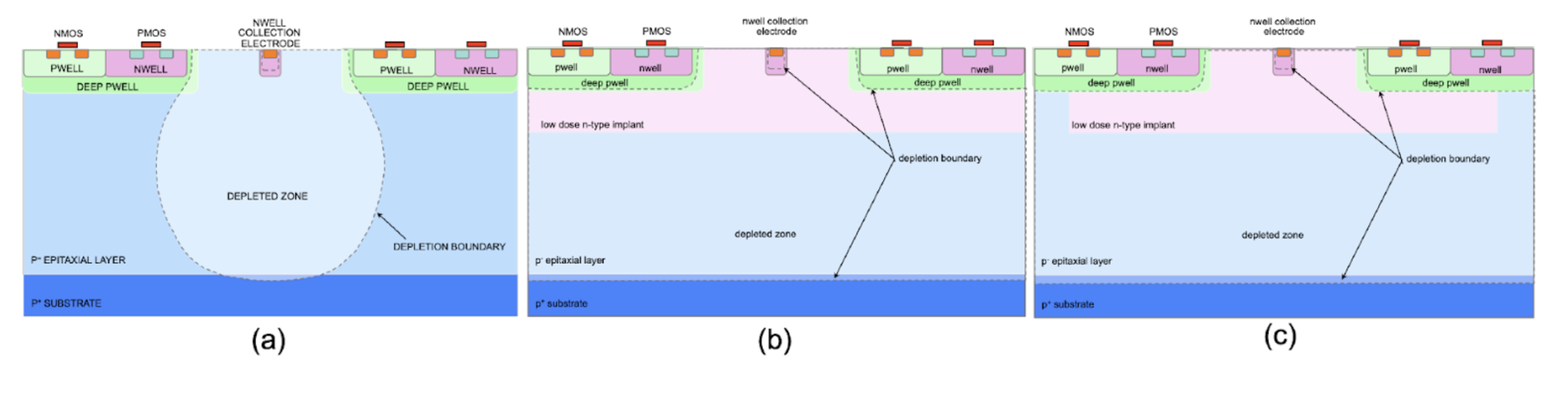
Figure 1: Cross-sections of three different pixel designs implemented both in 180 nm and 65 nm: (a) standard, also used in ALPIDE, (b) modified: with deep blanket low dose n-type implant, and (c) modified with gap: with gap in the same implant.
After the chips returned from the foundry, an intense testing campaign followed during the second half of 2021 and 2022. The results of this phase demonstrated that this technology can detect particles and withstand levels of radiation significantly exceeding the requirements of ITS3. Results from these first sensors in 65nm technology are at least comparable, if not better, to those obtained on the 180 nm technology. In particular, they show a sensor time resolution around 70 ps for small pixel pitches, and a detection efficiency maintained around 99% after fluences of 1015 1 MeV neq/cm2 – at room temperature, see Figure 2, opening perspectives for tolerance to even larger fluences when cooled. The result shown in Figure 2 was obtained on the Digital Pixel Test Structure or DPTS, which contains a 32 x 32 pixel matrix at 15 micron pitch, with each pixel equipped with analog front end and digital readout. The experimental results confirm the influence of the pixel design on the charge collection, and illustrate that the principles on which these pixel designs are based can be generally applied to different technologies. Specifically, pixel designs with the low dose n-type implant with and without gap suppress charge sharing significantly. The effect is more prominent in the version with a gap, resulting in a much more pronounced iron peak, practically independent of the pixel pitch. This remarkable feature provides the margin for full efficiency at larger pixel pitches, before as well as after irradiation.

Figure 2. DPTS efficiency and fake hit rate vs threshold before irradiation and after different irradiation levels.
The evaluation of the MLR1 chips is now being completed, and resulted in several conference presentations and proceedings, but also in some summarizing papers, including one on the Digital Pixel Test Structure. Another one on the Analog Pixel Test Structure or APTS aimed at studying the charge collection is being finalized.
The second submission in the WP1.2 framework, ER1, completed at the end of 2022, focused on the exploration of stitching. In standard CMOS manufacturing, the maximum size of a chip is limited to the reticle area defined by the field of view of the photolithographic process, typically a few centimeters in both directions. The special technique of stitching allows the manufacturing of chips, or MAPS in this case, larger than a single reticle, even up to 21 cm × 21 cm in size for 300 mm diameter wafers. The only limit is the size of the wafer. To achieve this, pieces of the chip smaller than the reticle are repeated multiple times, assembled or ‘stitched’ together on the wafer to form the larger chip.
Moreover, reducing the thickness of such wafer-scale sensors to values of about 20–40 µm opens the possibility of exploiting the flexible nature of silicon to implement large-area curved sensors. This makes it possible to build a cylindrical layer of silicon-only sensors, with a further significant reduction of the material thickness. This is pursued for the ALICE ITS3 upgrade, aiming to manufacture chips reaching the dimensions of 27 cm × 9 cm on silicon wafers of 300 mm diameter.

Figure 3. The ER1 submission contained two stitched sensors, MOSS and MOST, both about 26 cm long. The wafer (left) contains 6 of each, and also test chips. The reticle is shown in the middle and a picture of a wafer on the right.
The ER1 submission included two stitched sensors, the so-called MOSS and MOST. The MOnolithic Stitched Sensor (MOSS) prototype chip is the largest of the two chips of the ER1 submission employing stitching, measuring 25.9 cm x 1.4 cm. MOSS is designed to explore the viability of the stitching technique to make a wafer scale monolithic pixel sensor, to learn how to engineer the interconnects for the distribution of supplies and signaling on a wafer size chip.. The second stitched chip submitted on ER1 is the MOnolithic Stitched sensor with Timing prototype or MOST. It measures 2.5 mm by 25.9 cm and contains 40 tightly packed matrices of 18 μm by 18 μm pixels, connected to a shared wafer-scale asynchronous readout. In a different approach of stitching, the power supply is much more granular, allowing the impact of potential defects in certain pixels of the chip to be reduced. Both chips are functional and will enable us to learn more about the yield and electrical performance of such a design including IR drops, leakage currents, noise distributions and spreads of characteristics. Further tests in the coming months will allow us to learn more about stitching and ways to further improve its use. While this intense testing effort continues, also the design of the MOSAIX, the first full prototype for the ALICE ITS3 upgrade, is in full swing with a submission in the ER2 run planned for the fall of 2024.

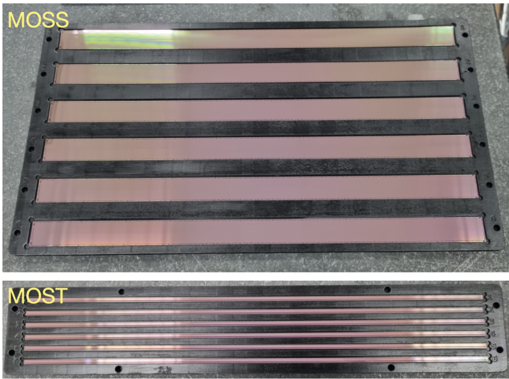
Figure 4. The left shows a special setup to extract the large MOSS and MOST chips from the wafer and place them in boxes shown on the right.
Advancing experience with stitching technology is admittedly an intensive R&D effort. This is a groundbreaking feature that WP1.2 members and the ALICE team working on ITS3 try to master and further advance. If successful, it could pave the application of MAPS for larger communities in many high-energy physics laboratories around the world as it could play a role in tracking detectors and vertex detectors, as well as in calorimetry.
Another important milestone achieved by the ALICE collaboration was the validation of the bending property of the Monolithic Active Pixel Sensors (MAPS). The first tests took place at DESY in June 2020 using 50 μm thick ALPIDE chips. The excellent performance figures of ALPIDE were retained after bending, proving that highly non-planar geometries become possible, profiting from the flexible nature of thin silicon. The bending technique has been optimized and several prototypes of bent detectors were brought to beam tests at DESY and CERN (both at PS and SPS beams), including a setup with three layers of ALPIDEs at the target radii of ITS3.
Tackling the complexity of these efforts and achieving reliable results calls for a collaborative effort. WP1.2 is acting as a hub for the LHC experimental groups. For Gianluca Aglieri Rinella and Walter Snoeys, coordinating the design effort, fostering synergies and creating interactions across different teams is a big part of their job and certainly important for succeeding in this mission. These goals were also met thanks to a strong and long-term working relationship established with the foundry. Successful collaboration for the ALPIDE chip and a history of previous orders in the 180 nm provided the entry ticket to the 65 nm technology, helping to build a relationship of mutual trust and professional understanding. This also allowed asking for certain modifications in the foundry’s manufacturing process, resulting in improving certain features of the chip like its radiation hardness and the signal collection speed.
These achievements testify to the approach to fulfill two key promises: the first concerns the very low material and ultra-light weight flexible integrated detector, and the second is to enable its use over large surfaces, profiting from the stitching technology. During these years, Aglieri recalls that the team often stepped from one difficulty to the other, but this has also been a learning trip. Thanks to these efforts, we have developed the needed skills and competencies in the group to overcome these difficulties, and this makes us optimistic about the prospects for the future success of these techniques.
This will be an important step not only for the ALICE ITS3 upgrade but also for other HEP experiments. Looking at longer time scales, the work of WP1.2 and the ALICE experiment is also progressing towards the goals set by ECFA for the detectors of a post-LHC collider. MAPS are also one of the few areas where production volume even within HEP is not negligible, which should help to access the most advanced technologies. More generally, large area pixel sensors are enabling devices for many cutting-edge research fields and practical applications. Fostering synergies and creating interactions across different teams is therefore not only essential to achieve the goals, but also beneficial for other fields.