In discussion with Michael Campbell: Unpacking the Medipix/Timepix Revolution

The Medipix and Timepix family of hybrid pixel detectors represents one of the most groundbreaking innovations to emerge from CERN's detector technology. These chips, based on the hybrid pixel technology developed for high-energy physics experiments, have found remarkable applications in diverse fields such as medical imaging, material science, and even space exploration. A recent article in the CERN Courier, "Watch out for hybrid pixels," highlights the immense potential and transformative impact of these technologies. In this interview, we delve deeper with Michael Campbell (MC) to explore the evolution of the Medipix/Timepix chips and their extraordinary journey from particle physics to real-world applications.
PC: The Medipix/Timepix family of chips has an extraordinary range of applications. Can you start by giving us a sense of the origins of this technology?
MC: Medipix and Timepix have been an incredible journey, evolving from hybrid pixel detector developments used as research tools for particle physics into versatile technologies with applications ranging from medical imaging to space exploration. The versatility of the ASICs and the ingenuity of our collaborating partners have been key to their success.
These chips originated from advancements in hybrid pixel detector technology at CERN, developed in the 1990s for the LHC. Work on hybrid pixel detectors started in the context of the LAA Collaboration as R&D for the LHC detectors, including the first pixel detectors for North Area experiments. This evolved into the RD19 collaboration and later the development of the ALICE silicon pixel detector.
For vertex-tracking detectors in HEP experiments, sequential frames of events are captured one at a time, with a single triggered frame being read out. As part of that early work, we tested the quality of bump bonding of our assemblies using radioactive sources, applying random triggers and adding up the images offline. We were creating X-ray images of our sources! This inspired us to implement a chip counting photons at the pixel level. The first informal Medipix collaboration, established in the mid-1990s, led to the first Medipix chip capable of counting individual X-ray photons in 1997.
PC: And this led ultimately to an impressive range of applications. Could you describe the first group of applications, perhaps chronologically?
MC: Initially, the goal was photon counting per pixel for X-ray applications, specifically for mammography. The first Medipix chip had a pixel size of 170 microns, which was too large for such applications, and had a matrix of only 64 x 64 pixels. While the chip didn’t make it into mammography machines, we were able to demonstrate that photon counting per pixel was feasible.
This led to the formation of the Medipix2 Collaboration in 1999 whose aim was to produce a chip for photon counting with much smaller pixels using the latest available CMOS process. The pixel size was reduced to 55 microns, the matrix size increased to 256 x 256, and the chips could be tiled on 3 sides. The first practical application was in X-ray diffraction. In 2001, Philips Analytical (later Malvern-Panalytical) signed a contract to use Medipix2 for X-ray diffraction, making them one of the first to market with a counting chip for X-ray diffractometers.
The major advantage of single-photon counting was its ability to produce noise-free images with a high dynamic range. The financial and technical support from Malvern-Panalytical was tremendously important for the continuation of our efforts.
Beyond industrial applications, Medipix2 was used as a platform to explore various sensor materials and topologies for X-ray radiography and other applications, including HEP. In 2010, I wrote a paper summarizing the work of the Medipix2 Collaboration to date and applications mentioned there include X-ray imaging, autoradiography, electron microscopy, and numerous others.
PC: But the Timepix chip was also developed in the context of the Medipix2 Collaboration. Can you describe how that came about?
MC: In 2005 members of the EUDET collaboration, in particular physicists from Nikhef and University of Bonn, asked the Medipix2 design team if we could adapt the Medipix2 chip using the clock not just for readout but also to record particle arrival times. The Medipix2 logic involves opening a shutter, counting hits asynchronously, closing it, and reading out using a clock. Instead of simply counting hits, they suggested using the same counter to record arrival times by counting clock ticks.
During the discussion, Xavier Llopart introduced the idea of measuring "time over threshold" as an alternative mode of operation. This led to the Timepix chip, capable of operating in three modes: single-photon counting, arrival-time measurement, or time-over-threshold. This flexibility opened the door to a wide range of new applications.
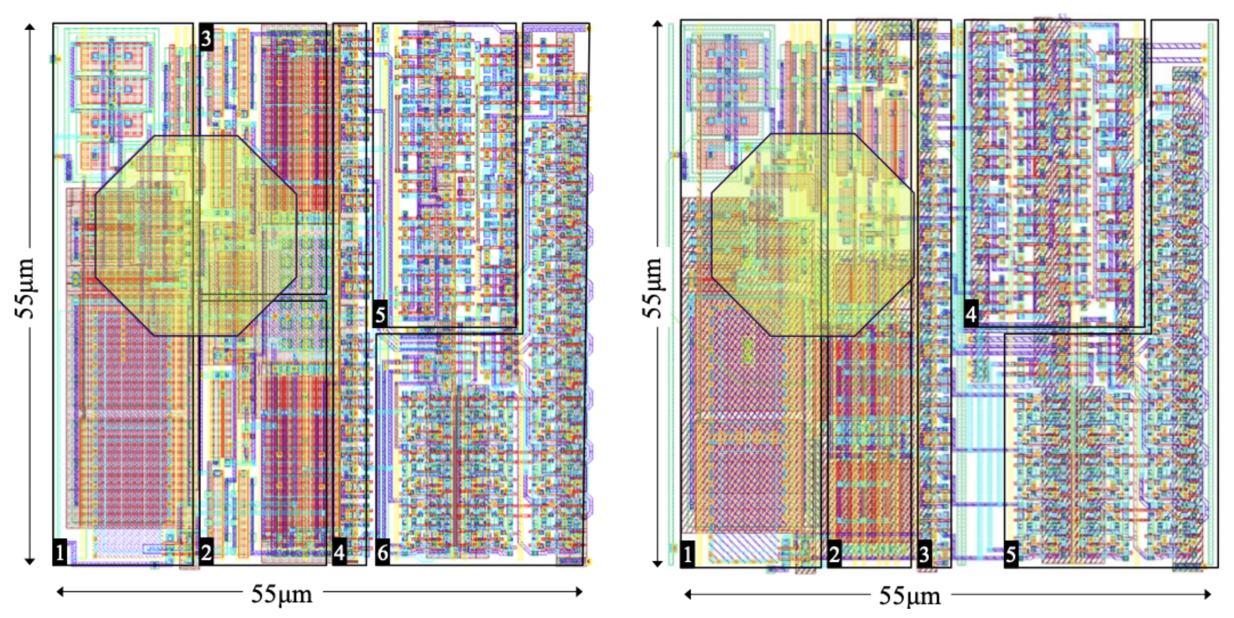
Layout of the Medipix2 pixel (left) and of the Timepix pixel (right) X. Llopart CERN-THESIS-2007-062
PC: Maybe a naive question, but moving from just counting single photons to adding these two extra functions—arrival times—how trivial was that?
MC: There’s a detail I didn’t mention. During the Medipix2 development, we started to explore spectroscopic imaging by having two discriminators on each pixel. However, measurements showed significant charge sharing, resulting in poor spectra for individual pixels, a problem we addressed later with Medipix3.
To move from Medipix2 to Timepix, we removed one discriminator and used the freed-up space to implement logic to allow selectable pixel operation modes. While the design change wasn’t a massive effort, the impact it had was huge.
PC: Nikhef and University of Bonn proposed this idea, leading to the development of these functionalities. Were they subsequently applied in experiments?
MC: Yes. Nikhef and University of Bonn have since been developing large-area gas detector readouts, basically TPCs, using Timepix in place of the pads used for readout in a gas detector TPC. They have installed a small area system for the CAST experiment and have built a large area prototype at DESY for the LPTPC Collaboration.
PC: With two ASICs now developed—Medipix2 and Timepix—what were the next steps in their evolution?
MC: After 2006, the Timepix and Medipix developments went kind of in parallel. The Medipix3 and Timepix3 chips were developed in the context of the Medipix3 Collaboration which started in 2005.
If I speak first about Medipix3, that's where Rafa Ballabriga joined the effort. As we had seen earlier with Medipix2, charge-sharing effects, including fluorescence in high-Z sensors, can lead to horribly dispersive X-ray images at small sensor pixel pitches. Together with Rafa and Xavi, we developed the concept of charge summing and allocation at the pixel level. We came up with an architecture that would do a local sum on the corner of every pixel and then allocate the hit to the pixel which had the most charge initially.
This cleans up the spectrum seen by an individual pixel. It's not perfectly clean because you add the noise of four pixels instead of one, but you still get a cleaner spectrum per pixel. For the Medipix3 chip, we also added other functionalities like continuous reading and writing.
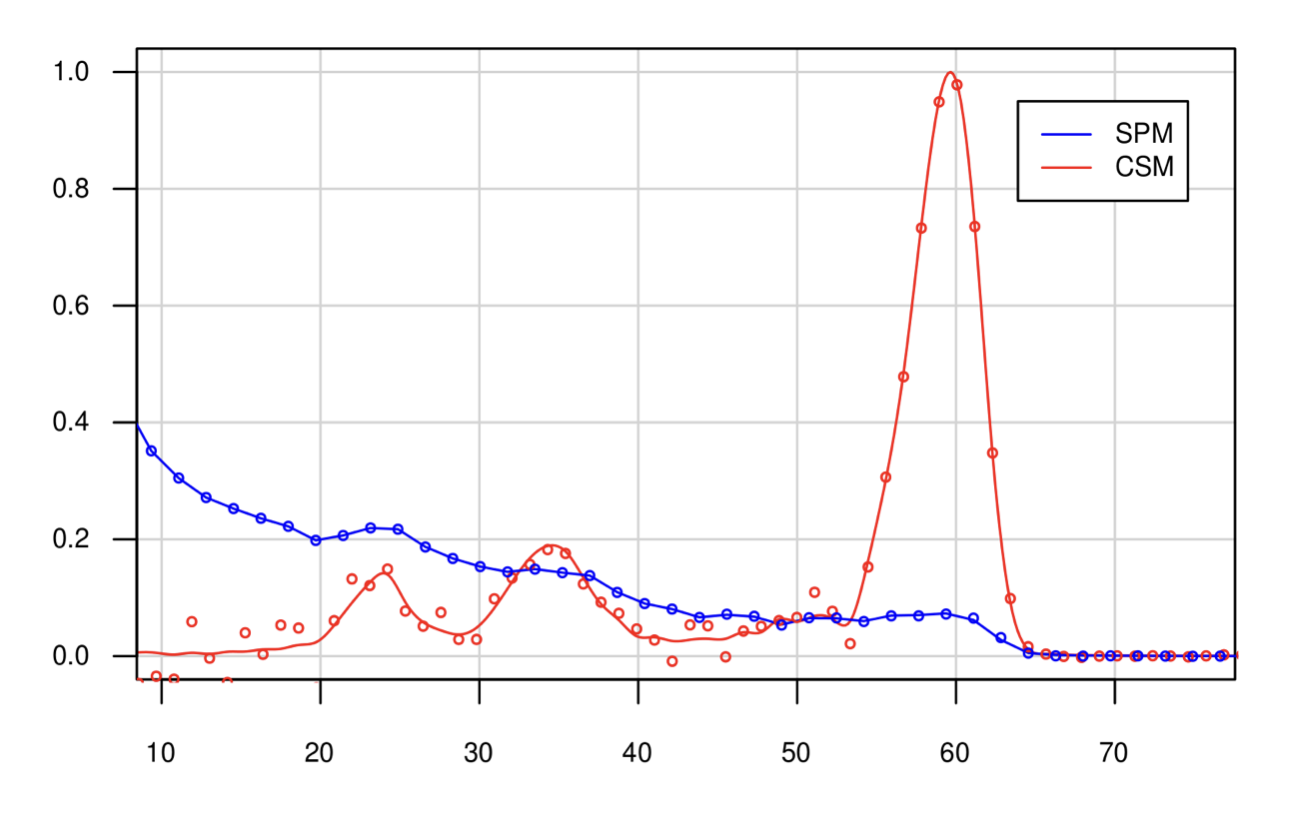
Comparison of 241Am spectrum measured with Medipix3 with charge summing and allocation logic off (blue) and on (red) T. Koenig et al., IEEE Trans. Nucl. Sci., vol. 60, no. 6, Dec. 2013.
We also added the functionality that you could take the same readout ASIC, connect it to a sensor with pixels of 55 microns or a sensor with 110-micron pitch, and still do the summing over 4 pixels of either 55 microns or 110 microns. This gave us a chip that was very flexible, adapted to silicon and gallium arsenide where the 55-micron pitch makes sense because of the internal fluorescence inside the sensor. Whereas for cadmium telluride, where the charge cloud is much more spread out, it made more sense to work with larger pixels.
In the Medipix3 chip, we had two thresholds per pixel. In spectroscopic mode, where we used the 110-micron pitch sensors, we could use the eight counters available on the four 55-micron pixels to get some kind of first spectroscopy. That's what we call spectroscopy mode.
PC: What were the key innovations introduced with Timepix3?
MC: The major leap from Timepix to Timepix3 was the adoption of a data-driven architecture. With the original Timepix, a significant limitation in the time-of-arrival mode was the depth of the counter. For example, the 14-bit counter on a pixel had a maximum count of 11,810 because of the pseudo-random counter architecture used. This meant that the shutter could only stay open in arrival-time mode for a duration determined by the clock period multiplied by this maximum count—imposing a major constraint. Moreover, in higher-rate environments, a pixel could be hit twice while the shutter was open, and the information about the second hit was lost.
With Timepix3, we overcame this by allowing each pixel to send information off-chip almost immediately after being hit. This approach only works if you have an excellent signal-to-noise ratio, which we ensure by setting thresholds well above the noise level. Typically, our chips operate at thresholds of between 500 and 1,000 electrons, with about 600 being the norm. Signals above this threshold are accurately detected, while anything below is ignored. In the Timepix3 design, we also improved the on-pixel timestamp resolution to a bin size of 1.6ns.
The simplicity of the chip’s behaviour is a testament to its efficiency. For example, if you place Timepix3 on a desk with no radiation source nearby, it remains silent—no data is output unless there's actual radiation to detect. This innovation not only solved the counter depth issue but also made Timepix3 more versatile and efficient for a wide range of applications.
PC: With Medipix3 and Timepix3 offering significant advancements, what key innovations did you introduce in the next generation, Timepix4?
MC: In Timepix4, we improved several features, most notably the timestamp resolution (you can watch a past EP seminar HERE). While Timepix3 achieved sub-clock tick resolution at 1.6 nanoseconds using a 40 MHz clock and a shared local oscillator between pixels, Timepix4 pushed this further to below 200 picoseconds. We also enhanced energy resolution, but the most impactful innovation was the novel floor plan. The chip's peripheral components are hidden beneath a regular matrix of bump-bonding pads, making the chip tileable on four sides. To achieve this, we designed two half-matrices of slightly rectangular pixels with a fan-out to a regular array of bump-bonding pads. Instead of reading out the chip through wire bonding pads at the bottom of the matrix, through silicon vias [TSVs] are used to bring signals to the rear of the chip. This design allows the chip to be diced right up to the edge, enabling nearly seamless tiling—a major breakthrough for large-area applications.
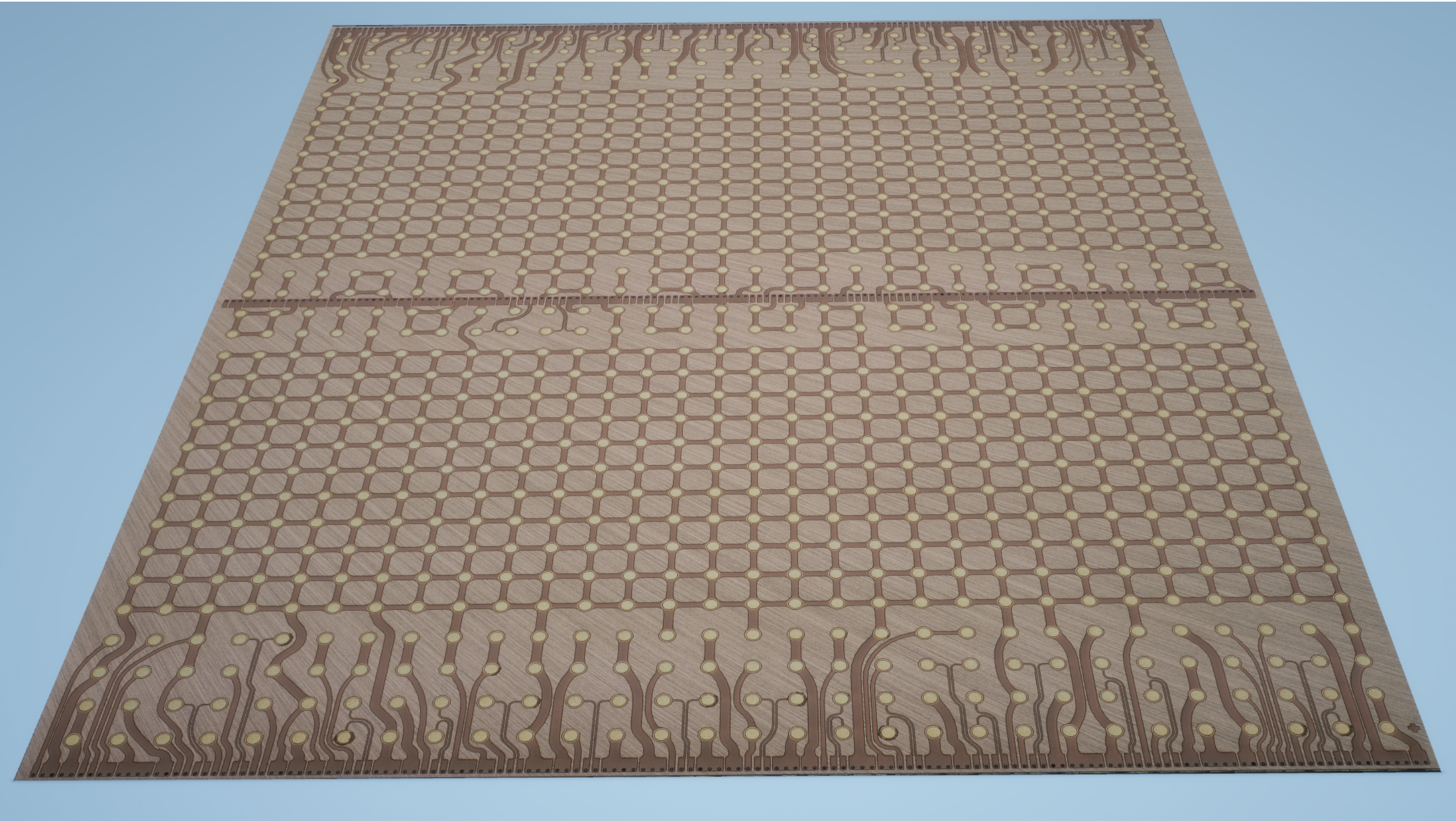
A rear side view of a Through Silicon Via (TSV) – processed Timepix4 chip. The chip design permits tiling on all four sides enabling large areas to be covered almost seamlessly. Photo: J. Alozy, CERN.
PC: What inspired the innovations in Timepix4, and how do they build on previous generations like Timepix3?
MC: The core motivation has always been to innovate and create something novel—to do something no one has done before. Timepix3 was the first data-driven pixelated chip on the market, and Timepix4 continues that tradition, cementing its position as a leader in this technology. The goal was to push the boundaries further, delivering better timing precision and the possibility of tiling large areas seamlessly.
These developments have also “spun back” to high-energy physics. Researchers from the LHCb experiment saw Timepix3's potential and requested adaptations to meet their requirements, leading to the development of the VELOpix readout chip by the same design team. The VELOpix detector is now running smoothly in the LHCb experiment, making a significant contribution to its physics reach.
PC: Beyond LHCb, how have Medipix and Timepix chips been applied in other physics experiments? Were there specific challenges or innovations that set them apart?
MC: The chips have been pivotal in other contexts. Timepix chips are used at ATLAS for precise radiation monitoring, creating detailed maps of radiation fields within detectors both during operation and when beams are off. In the UA9 experiment, Timepix chips are essential for beam monitoring, enabling precise measurements of beam profiles and dynamics in studies involving bent crystals for beam collimation.
Moreover, groundbreaking studies like positron annihilation in the AEGIS and ASACUSA experiments have relied on the exceptional timing and data capabilities of Timepix3. These examples underscore the adaptability of the technology for diverse physics applications.
PC: The latest Timepix chips can generate large data volumes in high-rate experiments. Managing such high data volumes must pose challenges. How do Timepix and Medipix handle this, and how do their use cases differ?
MC: Data volume is indeed a challenge. For example, placing Medipix3 in an X-ray beam and taking a single one-second exposure results in an image containing only tens of kilobytes of data. By contrast, placing Timepix3 in the same scenario generates hundreds of megabytes, as it captures x, y position, amplitude, and precise timing (1.6 nanoseconds) for each detected particle.
Timepix3’s richer data set makes it far more versatile than Medipix3, which excels in spectroscopic imaging for X-rays. While Medipix3 is more widely used in large-area detectors and sells more units—about ten times more historically—Timepix3 has significantly more research publications due to its broader applicability. Its flexibility has enabled breakthroughs in medical imaging, neutron detection, and particle tracking, making it indispensable in fields beyond X-ray imaging.
PC: The list of use cases is quite extensive. Could you highlight a few that best exemplify the impact of these chips?
MC: Certainly. One example is the Timepix3Cam, developed by one of our licensees, Amsterdam Scientific Instruments (ASI). It integrates the Timepix3 chip with a visible-light-sensitive sensor and an image intensifier, creating a camera that streams optical hit data. This system has been used in numerous scientific applications, including quantum science.
One particularly interesting application for physics was in the ARIADNE experiment. A camera from ASI was acquired by Liverpool University to read out bi-phase argon detector prototypes for DUNE. Here, liquid argon in a tank transitions to a gas phase, where a GEM (Gas Electron Multiplier) amplifies charges, producing bursts of photons. The Timepix3Cam captures the x, y position and timing of these photons, allowing real-time imaging of detector events. Reading out the detector in the optical regime eliminates the need for cryogenic electronics and lenses can be used to focus large-area images onto smaller detectors.
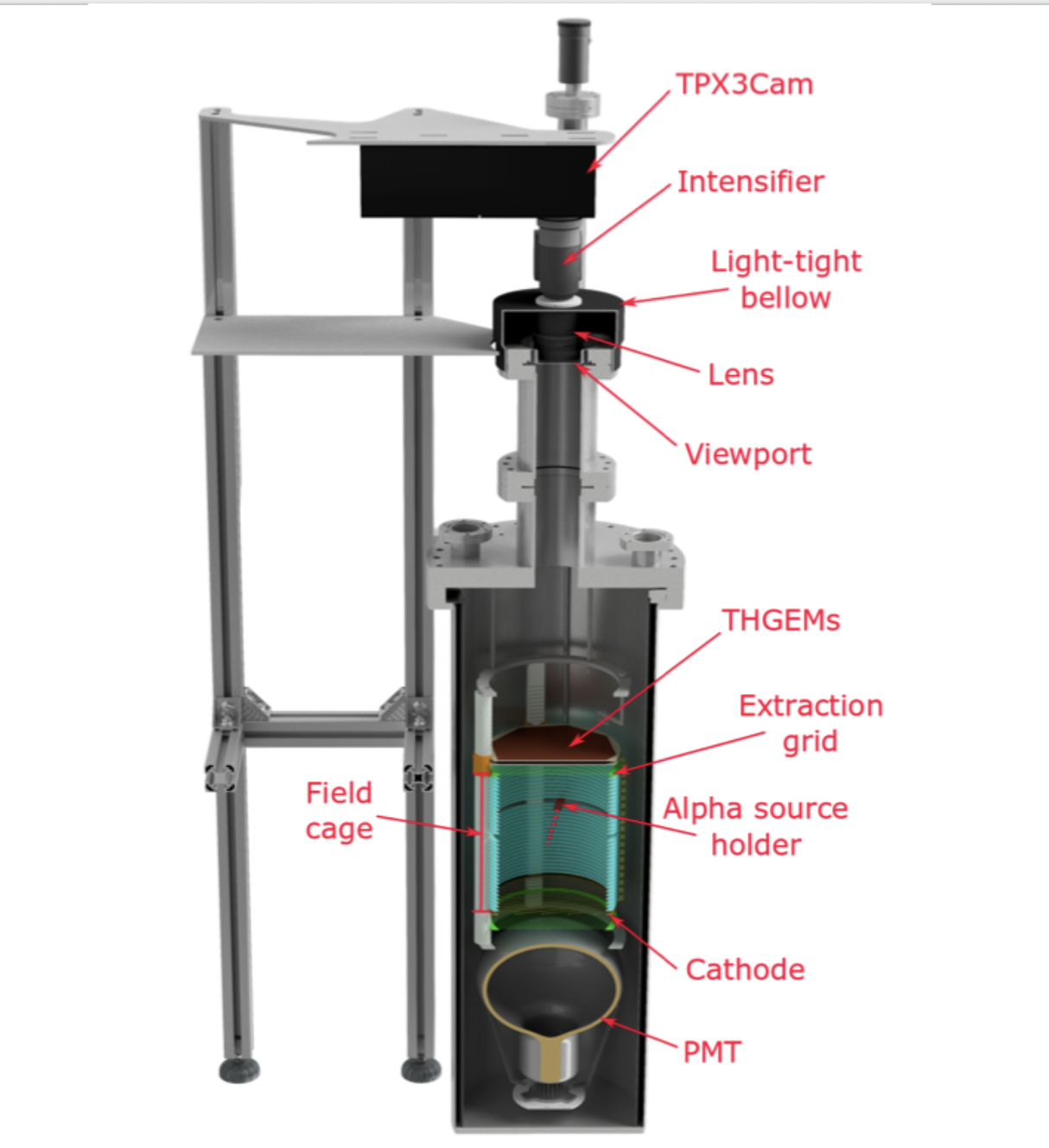
The TPIX3Cam streams out hits from photons generated in a thick GEM. This is a prototype for the ARIADNE neutrino detector readout A. Roberts et al 2019 JINST 14 P06001.
Another significant example is in medical imaging, where Medipix3 was incorporated into a scanner by MARS Bioimaging in New Zealand in the 2010s. Despite challenges with regulatory approvals and funding, they succeeded in producing world-class imaging systems. In this case, the Medipix3 Collaboration granted MARS an exclusive license to exploit Medipix3 in the medical CT field. This license enabled them to raise the large funds needed to bring Medipix3 from the lab to the clinic.
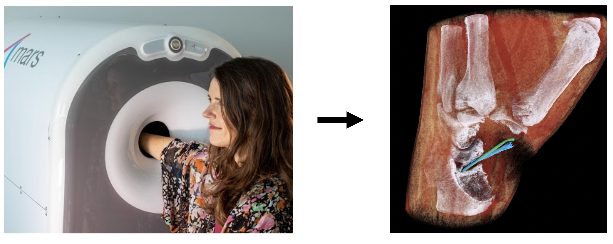
The MARS wrist scanner, based on a Medipix3 camera, provides high-resolution images with tissue discrimination, even in the presence of metal implants.
The chips have also been used in the development of a Compton camera for thyroid imaging based on Timepix3, funded through European grants.
I’d like to stress that it is the commercial licensees of our technologies who enable dissemination into many new fields. Neither CERN nor our academic collaboration partners would have the resources to make such an impact.
PC: You mentioned that one of the things you are proud of is that the Timepix chip can be found both in space and in the classroom. What do you mean by that?
MC: Essentially, the same core technology used in cutting-edge space research is now accessible for students. In 2013, Advacam introduced a classroom-friendly kit, the MiniPIX EDU, in Prague. This device, based on the Timepix chip, allows students to detect and visualize ionizing radiation in real time by simply connecting it to a computer via USB. Using intuitive software, they can observe alpha, beta, and gamma particles, creating distinct traces on the detector, providing immediate, hands-on insights into radiation. It’s also a great way to introduce students to computer-aided data analysis. A handbook was developed by the Institute of Experimental and Applied Physics in Prague (IEAP) to guide teachers in its use. These kinds of experiments engage students with practical, hands-on learning, while also highlighting the real-world relevance of science.
One of the most compelling aspects of the MiniPIX EDU for high school students is its connection to advanced science. A more advanced implementation of the same technology is used in the International Space Station. Following groundbreaking work by IEAP and the University of Houston, NASA adopted Timepix for regular use as a dosimeter for manned space flight missions. Students have been able to access data from the space station and from various space weather satellites. The same Timepix device they used in their classrooms flew on the Artemis 1 test flight and, most recently, was discretely monitoring the doses received by the first SpaceX tourists as they flew through the Van Allen Belts. My favourite device, though, is the ‘lonely’ one which was released into interplanetary space during the Artemis 1 flight on the Biosentinal CubeSat. It is about 50 million km from Earth and is still reporting regularly on space weather to Earth. Imagining the view from that device helps me put our earthly trials and tribulations into perspective!
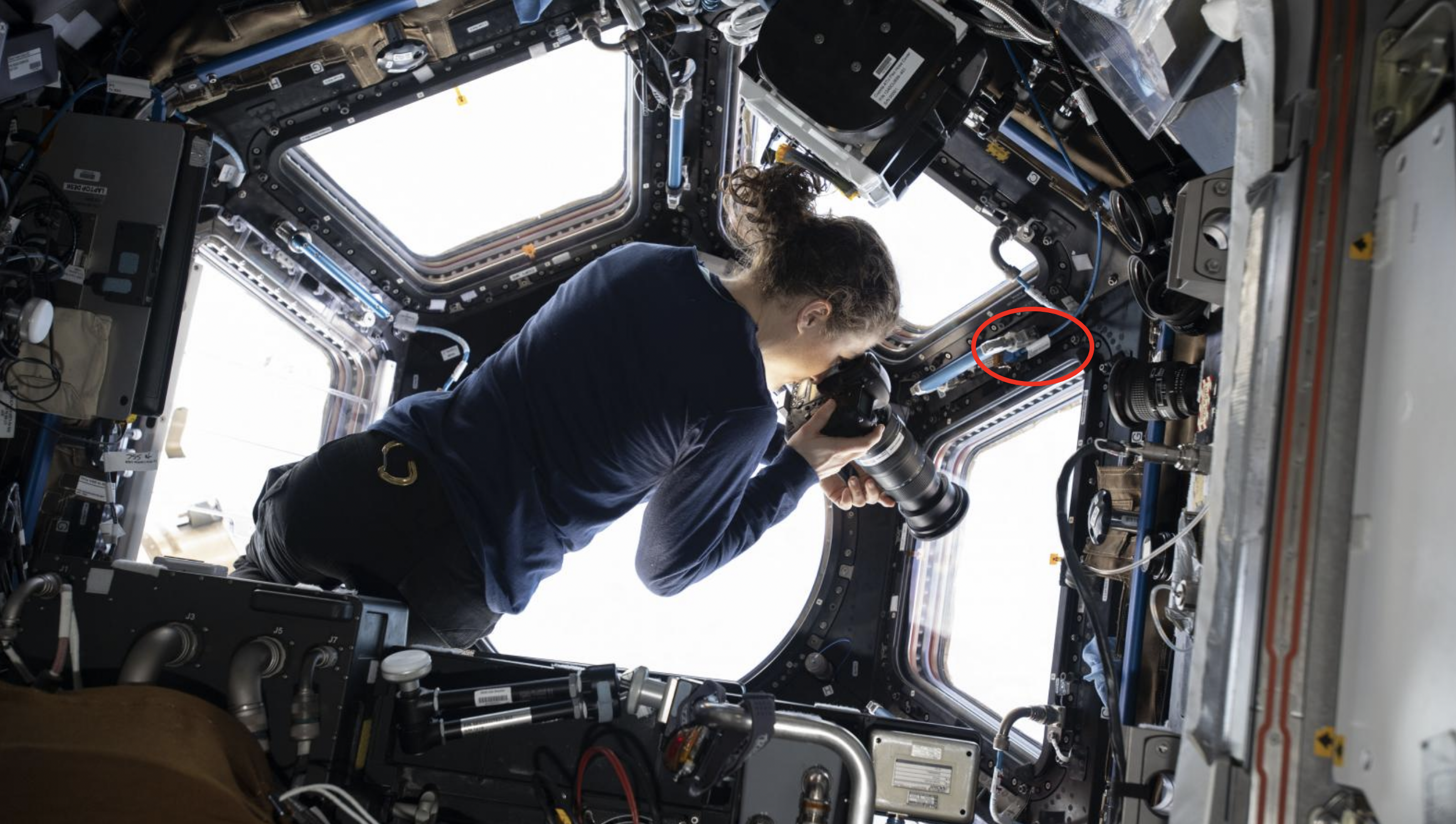
An astronaut photographing earth from the cupola of the International Space Station. The Timepix device (circled in red) is recording the radiation dose of the crew. Photo courtesy of NASA.
The MiniPix system can also just be fun to use. I sometimes use in on a plane partly to remind myself why I should fly less. I also once surprised a rather wealthy friend who lives in a palace in the historical centre of Rome by showing him how much radioactivity is emitted by the granite blocks used to create such beautiful buildings.
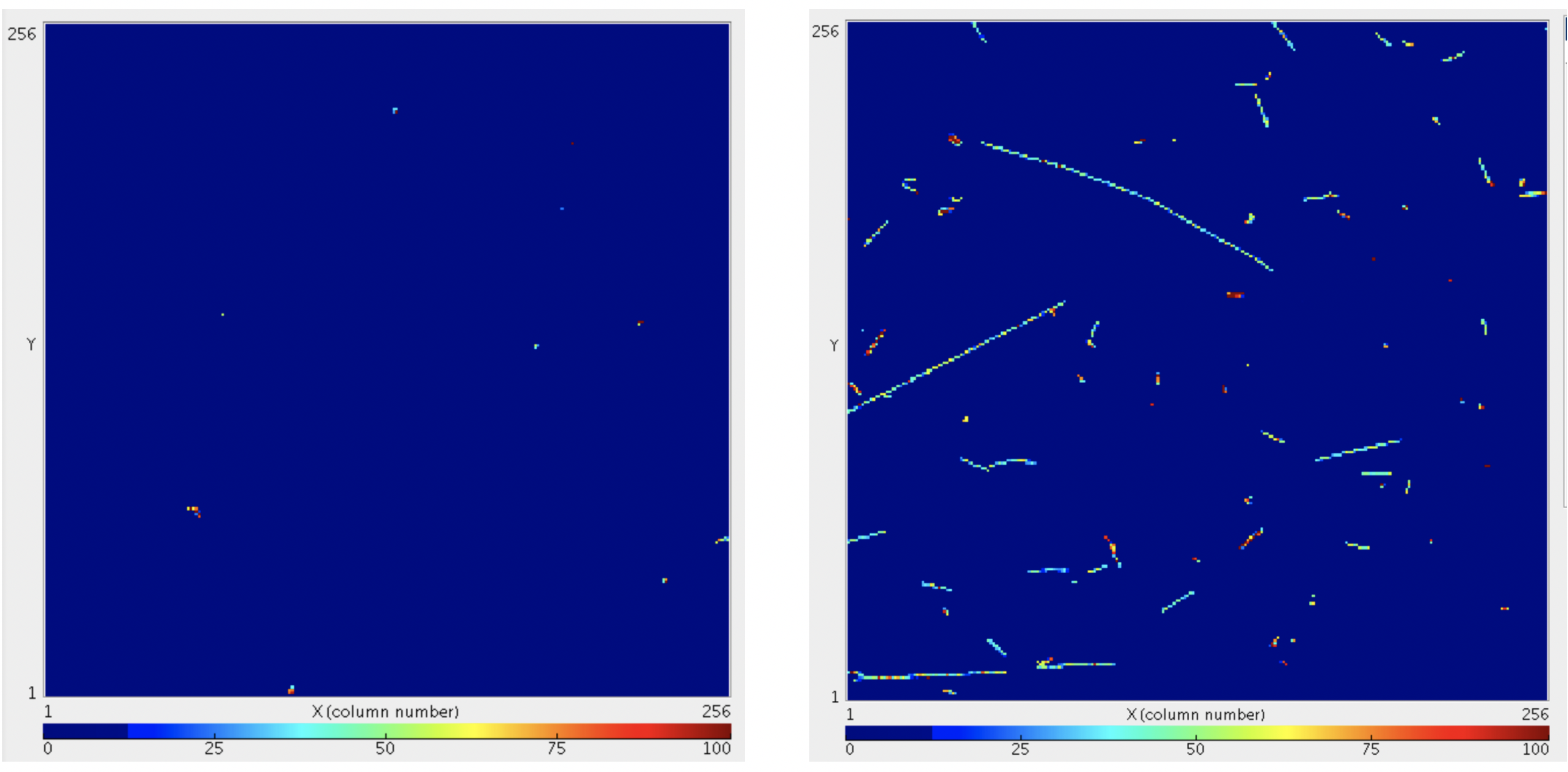
Frames showing a recording of background radiation by Timepix over a 1 minute exposure time. The left frame was taken at a location near to sea level. The right frame was taken while flying at a cruising altitude of ~35 000ft.
Pilot programs in the UK and Barcelona have shown that this approach significantly boosts interest in physics, particularly among teenage girls—a demographic often lost to STEM fields. To expand its reach, a new CERN & Society project aims to distribute these kits globally, creating local hubs with curriculum-aligned resources to ensure widespread accessibility. This initiative supports a broader goal: fostering the STEM-educated workforce essential for the future of hi-tech industries.
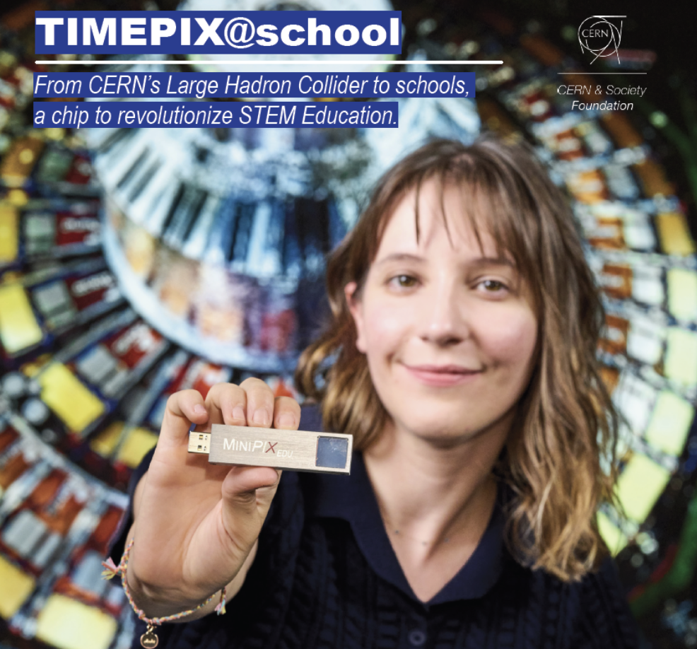
Successful pilot projects in the UK, Spain, and beyond have shown that this groundbreaking technology not only sparks high school students' (especially girls') interest in STEM but also boosts teachers' motivation. By inspiring the next generation, TIMEPIX plays a key role in shaping the future of the microelectronics industry. The CERN & Society Foundation is working to bring this innovative tool to more schools worldwide.
PC: Can you think of an application that you have not yet seen but would like to see explored?
MC: One idea that intrigues me, particularly with the advancements in Timepix3 and Timepix4, is leveraging their ability to track within the sensor itself. With these chips, you can observe track stubs within the silicon, similar to what you might see in a TPC gas detector because the charge collection is tagged with a timing resolution of down to 200 picoseconds. This means that instead of just getting a single point in space, you can reconstruct a short segment of the particle's trajectory from a single plane.
This capability remains largely unexploited by the physics community although there has been pioneering work by our Czech colleagues from IEAP in the MoEDAL experiment. Traditionally, trackers are built with very thin planes placed sequentially, and you reconstruct tracks by joining dots across layers. Calorimeters, on the other hand, are designed to stop particles entirely and measure their energy deposition. But with the vector information we can now obtain from a single plane of our detectors, there’s an opportunity to rethink this approach.
Imagine using a single, trigger-free detector with continuous sensitivity to track and reconstruct particle paths in a new way. It could blur the lines between traditional tracking and calorimetry, offering richer data from fewer components. This shift in thinking could open up new possibilities for more compact and efficient detector designs in future experiments.
PC: How has CERN's EP department supported the development of the Medipix and Timepix projects?
MC: The EP department at CERN has been crucial and supportive, even though we've mostly operated under a model of "tolerated existence," meaning we had to rely almost exclusively on external resources. A key factor in our success has been the Medipix Collaborations that funded our design manpower. While EP covered a portion of my salary, the Collaborations were instrumental in supporting our designers.
However, EP's contribution goes beyond just financial support. It has provided us with invaluable technical infrastructure, including access to top-notch engineers, software design tools, lab space, and essential administrative support. Beyond EP, CERN's expertise in areas like contract writing, collaboration agreements, and negotiating with foundries has been crucial. The KT group has also been an essential player in licensing our chips.
We've also benefited significantly from CERN's central role in the high-energy physics community, particularly in microelectronics design.
I see it as a mutually beneficial relationship. While we've received vital support from CERN, we've also contributed by generating positive publicity for the organization and demonstrating the broader relevance of the work of the HEP community in microelectronics to other fields.
PC: How have CERN and the EP department contributed to the broader adoption of technologies like photon counting and other applications of Medipix/Timepix?
MC: I think one of CERN’s unique strengths is its ability to serve as a neutral, collaborative platform that brings together diverse stakeholders to address shared challenges. For example, in the context of photon counting, the workshop we’ve organized every two years has been instrumental in moving this technology from the lab into clinical applications. While companies like Siemens were the first to bring photon counting scanners to the market, CERN played a vital role in facilitating and encouraging the early discussions that helped make this possible.
In 2011, with crucial support from Patricia Mage and her collaborators, CERN hosted the first workshop on Medical Applications of Spectroscopic X-ray Detectors. At that time, even the feasibility of photon counting in medicine was open to question, never mind any potential clinical benefits. At these workshops, we were able to attract leading companies and their technical experts for in-depth scientific discussions. The neutral ground of CERN allowed for open and productive exchanges without the need for sign-offs from marketing departments or other bureaucratic hurdles. This openness and focus on problem-solving helped the community collectively address the challenges of integrating photon-counting technology into clinical scanners.
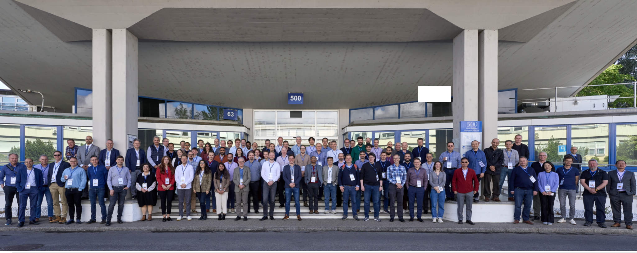
Group photo from the 7th Workshop on Medical Applications of Spectroscopic X-ray Detectors, where the world's leading medical equipment suppliers joined forces with top research institutes. Building on the foundations laid at the 1st workshop, the Medipix Collaboration continues to play a pathfinding role in shaping the future of this cutting-edge field.
Beyond that, our Medipix collaboration meetings, held four times a year, play a crucial role in fostering innovation. These meetings bring together people working on diverse topics, creating a space for exchanging ideas and learning about applications outside their immediate focus. It’s this cross-pollination of ideas that often leads to breakthroughs. Whether it’s photon counting or other applications, I’m very proud of how these forums have contributed to the ecosystem of innovation around Medipix and Timepix. CERN’s role in enabling this open, collaborative environment has been essential for moving these technologies forward.
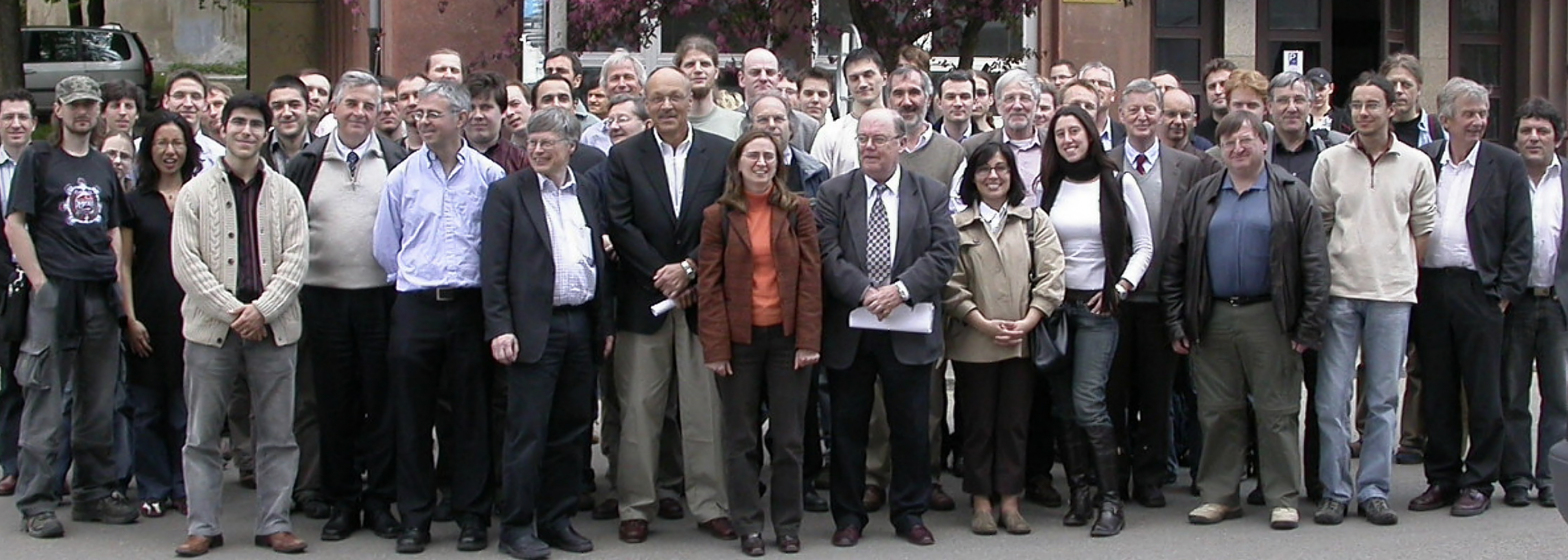
Photo taken at Medipix Collaboration meeting at IEAP Prague, May 2009.
PC: What concerns you most about the future of the Medipix and Timepix projects?
MC: I have two main concerns. First, as the complexity of the chips increases, so do the demands on resources and funding. Up until now, we’ve relied on the Collaboration to pool the money needed to pay the engineers who design the chips and to fund the production runs. However, this model might not be sustainable in the future without CERN committing significantly more resources than it has in the past. The engineering design team is already small and tightly knit, and their responsibilities have increased in the last few years. Adding to their workload without additional support would be incredibly challenging.
Second, there’s the issue of managing the organizational side of the project. For years, I’ve taken on many of those responsibilities, but as I step back from being in the driving seat towards the end of 2025, those tasks will inevitably fall to the designers. Balancing their technical design work with the increased organizational responsibilities will be tough. My goal is to support them as much as I can—I’ll be in the passenger seat, so to speak—but they’ll need additional resources and structural support to keep the project moving forward effectively. These challenges will need careful consideration to ensure the long-term success of the Medipix and Timepix developments.
PC: To conclude this interview, I’d like to ask about the future. What do you envision for the next steps beyond Timepix4?
MC: Timepix4 is still being tested, but it’s already proving to be a significant success. It has advanced capabilities, and while some improvements or bug fixes would be ideal, the cost of a rerun is very high, and we’re currently struggling to raise the necessary funds for that. On the Medipix side, the interest in Medipix4 has been more limited so far, but I’m confident that once it becomes available, it be used in applications requiring larger areas than those of Timepix4. Medipix4 has all the hallmarks of a successful chip—it’s just not fully tested yet.
Looking ahead, we’re exploring the next steps, with Xavi working on a project called LA-PicoPix, which could be considered a precursor to Timepix5. This effort focuses on integrating more intelligence directly into the chip, both at the pixel matrix level and in its periphery, to manage the enormous data flow generated by these advanced detectors. The goal is to implement processors on the chip that can selectively filter and process data in real-time—identifying, clustering, and even rejecting events based on specific criteria. By improving the data package format and adding this level of intelligence, we hope to make the detectors more efficient and capable of handling the increasing complexity of data in high-energy physics and beyond. The path to Timepix5 is clear, but the challenges of resources and support remain. If we can secure sufficient backing from CERN and our partners, I’m optimistic about what might lie ahead.
