![]()
MOSAIX: Designing bent wafer-scale monolithic pixel sensors for the ALICE ITS3 upgrade

The ALICE detector is preparing a major upgrade to its Inner Tracking System (ITS) during LHC long shutdown 3 (2026-2030). This upgrade, called ITS3, will replace the three innermost tracking layers with three layers of cylindrical, 50 µm thick, 27 cm long, silicon sensors bent around the beam pipe.
The primary goals are to reduce the material budget from 0.36% X0 to 0.09% X0 per layer and to position the first layer of the detector just 19 mm away from the interaction point, much closer than the 24 mm of the existing ITS2. This will enhance the pointing resolution with which the ITS can measure the origin or vertex of particles by a factor of 2, which is particularly relevant for low-momentum particles.
The monolithic sensors, measuring up to 27 x 10 cm2, integrate sensitive area and peripheral circuitry on the same die. They are bent around the beam pipe and are sufficiently stable to be held in place only by carbon foam spacers, thus avoiding heavy support structures. The sensor also directly integrates power distribution and data communication, with no need for external cables placed in the sensitive detector area. Air cooling instead of water cooling is employed to reduce the material in the active area even further. The core challenge of this project is therefore developing a silicon-only, wafer-scale, monolithic stitched pixel sensor compatible with bending, consuming no more than 40 mW/cm2 of power, and capable of transmitting data rates of up to 30.72 Gb/s. Furthermore, the impact of unavoidable silicon sensor manufacturing defects is mitigated by a modular implementation, which allows switching off defective areas. Figure 1 shows a comparison between the ITS2 half inner barrel and an ITS3 half inner barrel mock-up.
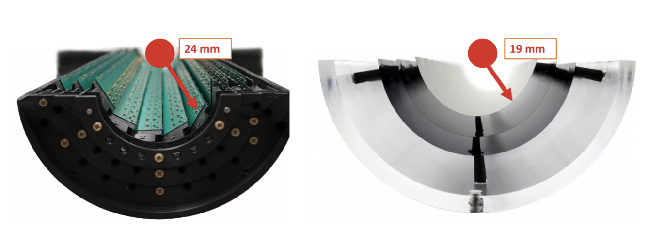
Figure 1. Comparison of the ITS2 half inner barrel, 24 mm from the beampipe, 0.36% X0 per layer and the ITS3 half inner barrel mock-up, 19 mm from the beampipe, 0.09% X0 per layer.
Stitching: Overcoming lithography limits
Standard semiconductor lithography generally restricts the maximum circuit area that can be fabricated in a single exposure to about 3 x 3 cm2 due to equipment limitations. However, with stitching technology, these individual areas can be seamlessly combined to form a continuous, wafer-scale chip. An example is shown in Figure 2, where the sensitive repeated sensor unit, A, is aligned and stitched together to form a larger sensitive area. This stitching approach requires carefully designed power distribution and data communication networks to ensure consistent functionality across the entire stitched area.
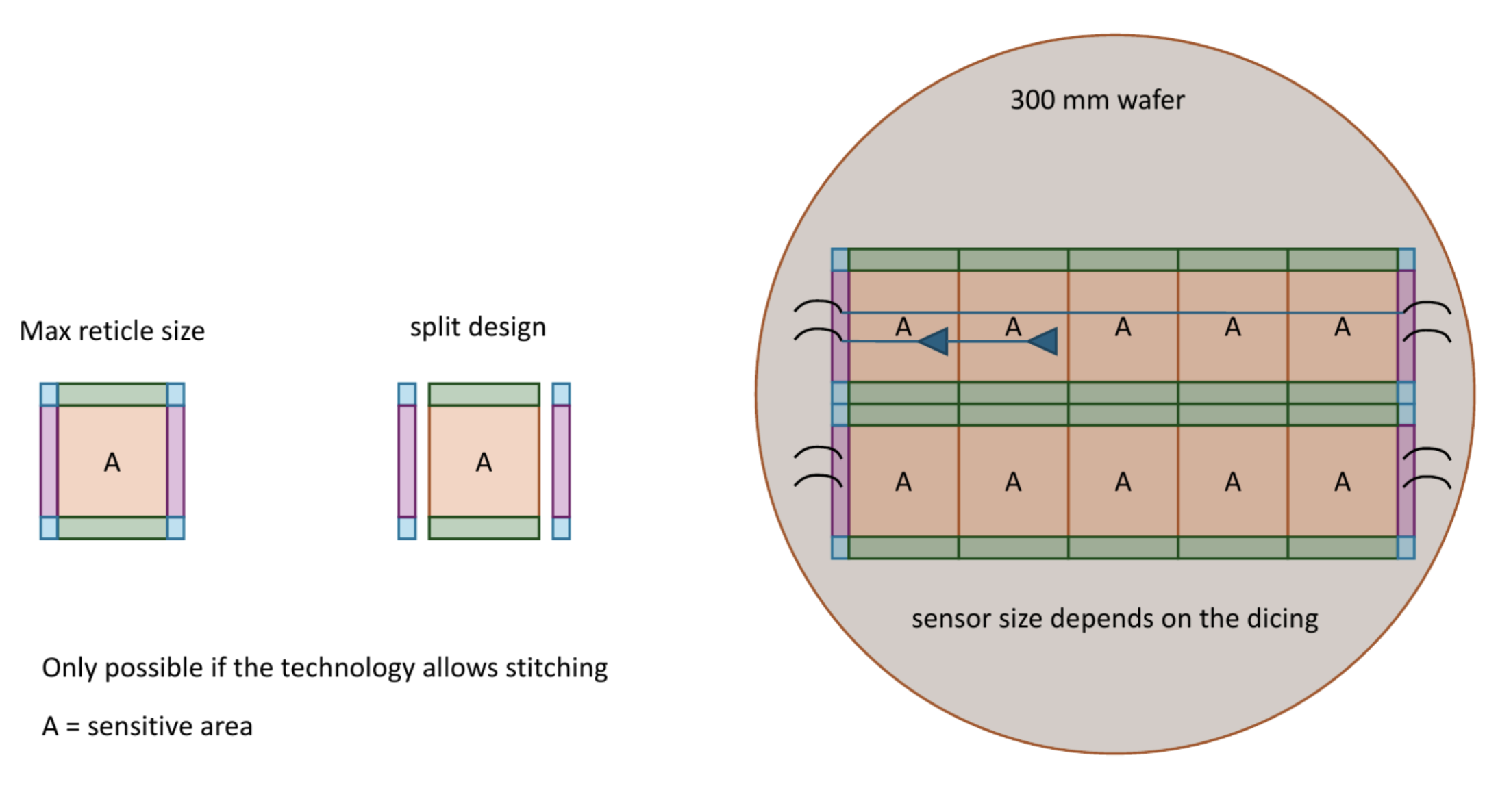
Figure 2 - Stitching example of a 300 mm wafer
The ALICE ITS3 detector
Figure 3 illustrates the structure of the ITS3 detector, with an exploded view of its layers shown on the left and the ITS3 sensor’s wafer map on the right. The 3 ITS3 layers comprise 3, 4 or 5 independent detector segments to achieve the necessary cylindrical sensor shape around the beam pipe. A segment is composed of 12 repeated sensor units and a readout processor at the so-called left end cap, all stitched together. This segmentation allows the entire detector to be built using the same photomasks from a single design, patterned onto only 6 wafers.
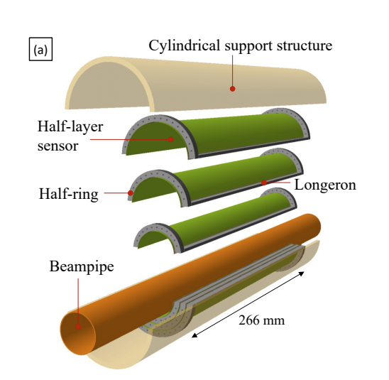
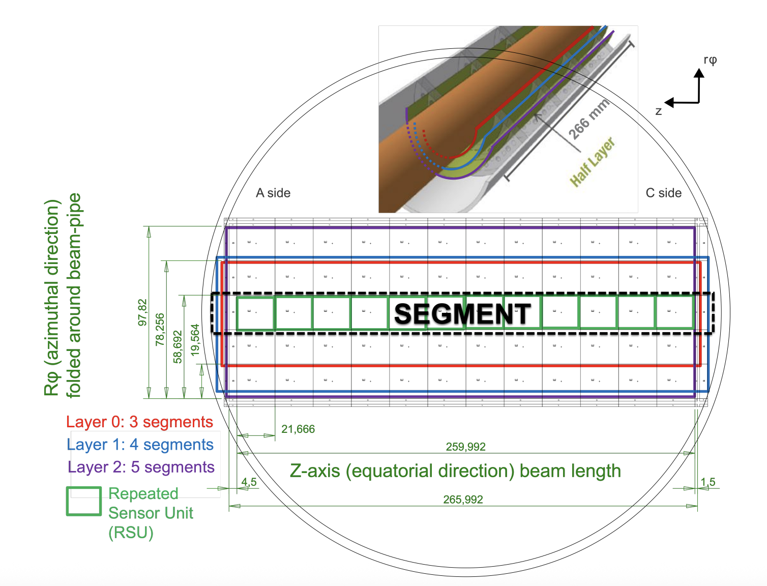
Figure 3. Top: Simplified ITS3 Detector layout, showing the 3 top and 3 bottom half layers around the beam pipe within the cylindrical support structure supported by carbon foam half-rings and longerons. Bottom: The three ITS3 layers comprise 3, 4 or 5 independent detector segments to achieve the necessary cylindrical sensor shape around the beam pipe. A segment is composed of 12 repeated sensor units and a readout processor at the so-called left end cap, all stitched together. This segmentation allows the entire detector to be built using the same photomasks from a single design, patterned onto only 6 wafers.
From the ALPIDE to Monolithic CMOS Pixels with Stitching
The technology of Monolithic Active Pixel Sensors (MAPS) is not new to ALICE. The current ITS2 detector, installed during LS2, was one of the pioneers in adopting the MAPS technology in a large scale by developing the ALPIDE sensor in a 180 nm CMOS imaging process, which covers nearly 10 m2 of the detector. The success of ALPIDE in ITS2 demonstrated the potential of MAPS in particle tracking, particularly since this technology exploits the fact that, unlike the conventional hybrid pixel detectors, the sensor diodes and the readout electronics are on the same die, contributing to a low material budget.
The journey towards the ITS3’s sensor has been driven by an intensive R&D program performed in the framework of the ALICE collaboration and the CERN EP R&D Work Package 1.2. The design team moved to a 65 nm CMOS imaging technology which offers smaller transistor dimensions and hence higher integration density and the ability to manufacture designs on 300 mm diameter wafers. R&D test sensors in this process were developed to qualify the 65 nm technology for the ITS3 application.
Two wafer-scale stitched pixel sensors were prototyped, the MOSS and MOST, measuring 26 x 1.4 cm2 and 26 x 0.25 cm2, respectively. Figure 4 shows the wafer . The prototypes were made to optimise the pixel performance and size, to study the stitching technique for 26 cm-long power and high-speed signal lines and to define a modular power delivery architecture to mitigate manufacturing defects in wafer production. Both prototypes confirmed the viability of such a pixel sensor for use in ITS3.
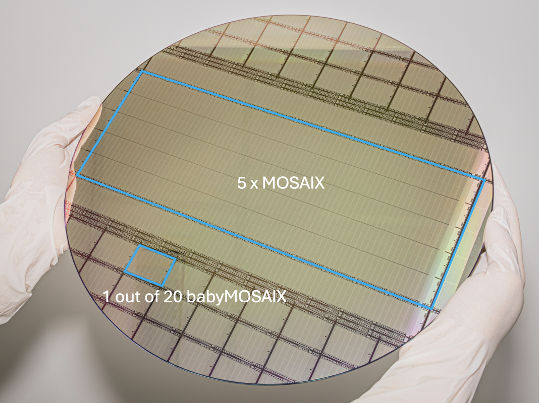
Figure 4: Engineering Run 2 wafer with five full-size MOSAIX sensor chips and 20 smaller babyMOSAIX prototype chips, used to validate key aspects of the ITS3 sensor design and production process.
The MOSAIX (MOnolithic Stitched Active pIXel) Wafer-Scale Pixel Chip
The culmination of the R&D effort is MOSAIX, the full-size, fully functional sensor prototype chip designed for the ITS3 detector. The name refers to a “mosaic” of pixel areas, or tiles, that illustrates both the chip's structure and operating principle. It measures 26.6 x 1.96 cm2, of which 93% is sensitive to particles, and is divided into 144 independently powered sensor tiles. This modular approach enables effective defect management by treating each tile as an independent unit for both power and data acquisition. Figure 5 shows the MOSAIX block diagram, highlighting the Left Endcap block, one of 12 Repeated Sensor Unit blocks with 12-pixel matrix tiles, each comprising a total of 10 million pixels, and the Right Endcap block.
Due to the mechanical constraints of the ITS3 detector, data and power can only be supplied via the short edges. The Right Endcap is only used for power connections. The hit data from every tile flows towards the Left Endcap, which acts as the chip's data hub and lies outside the detector's acceptance area. Each sensor tile transmits on-chip-packaged hit data differentially at 160 Mb/s via a point-to-point connection to the Left Endcap. The tile data is aggregated and sent to the counting room via the 10.24 Gb/s trasnmitters.
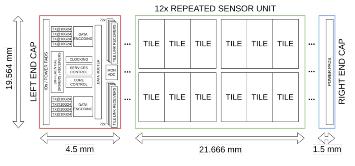
Figure 5: MOSAIX block diagram.
The MOSAIX design integrates functionality that would previously often be implemented across several ASICs assembled on a hybrid carrier. In MOSAIX, all these functions are implemented within a single ASIC. Developments of this complexity are traditionally carried out in stages, with individual components tested separately before being integrated and validated together on a hybrid board. Great care was taken in both design and verification prior to ASIC production, including thorough simulation of individual building blocks, their integration, and their system-level interactions.
A total of 36 MOSAIX wafers were delivered in February 2026. The MOSAIX testing phase was prepared almost a year prior to delivery, conceived to carefully test the multiple functional blocks embedded in the sensor. Before MOSAIX became available, functional models implemented in a programmable emulator were used to design and validate the test system hardware, firmware, and software. The test platform, based on an FPGA-processor architecture, was therefore fully prepared in advance. As a result, once MOSAIX was delivered, the chip could be integrated into the test system within hours, enabling immediate functional verification.
The tests have demonstrated the overall functionality of MOSAIX, while yield and performance characterisation in both laboratory and beam-test environments are ongoing. These studies have already provided valuable feedback that is being used to optimise the final production version of the MOSAIX sensor. Figure 6 shows MOSAIX detecting beam particles within an ALPIDE-based beam telescope setup, while Figure 7 demonstrates the correct operation of the MOSAIX high-speed data serializer.
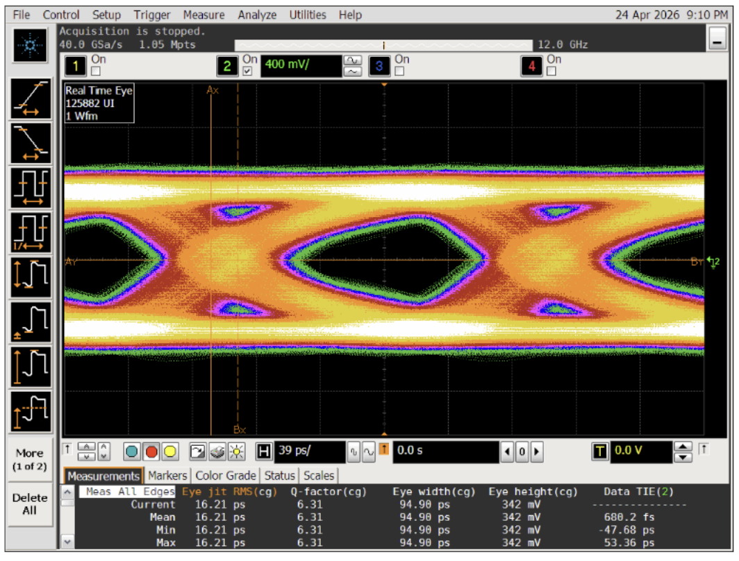
Figure 6: Testing of a 5 Gbit/s serializer data stream with a high-speed vertical needle probe card.
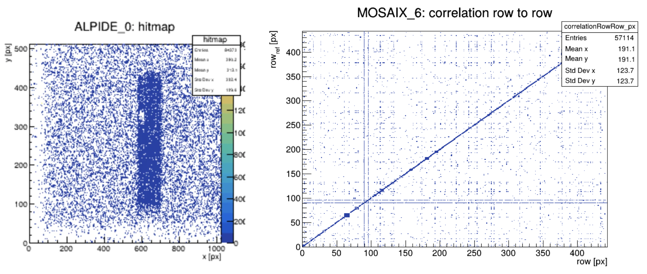
Figure 7: MOSAIX detects beam particles in ALPIDE beam telescope; overlay plot of MOSAIX hits with ALPIDE telescope hits (left); correlation plot row by row (right)
MOSAIX represents an unprecedented level of complexity and pioneering advancements in detector technology by employing 50 µm thin wafer-scale sensors and stitching techniques to build wafer-scale sensors with minimal material budget.
Further reading
- Technical Design Report for the ALICE Inner Tracking System 3 - ITS3; A bent wafer-scale monolithic pixel detector
- https://ep-news.web.cern.ch/content/pushing-boundaries-monolithic-cmos-sensor-technologies
- https://ep-news.web.cern.ch/content/ultralight-air-cooled-mechanics-alice-its3
- https://ep-news.web.cern.ch/content/its3-and-focal-two-new-subdetectors-extend-alices-physics-reach
- https://iopscience.iop.org/article/10.1088/1748-0221/20/06/C06001
- https://iopscience.iop.org/article/10.1088/1748-0221/20/02/C02015