![]()
25 years of Microelectronics at CERN: from LAA to the LHC
Last November, the success of the LAA R&D project that led to the development of microelectronics at CERN was celebrated. LAA was a well-defined R&D activity for the study of new detection techniques for the next generation of hadron-colliders that would reach the scale of TeVs.
In a special event at CERN, some of the first members of the project met and shared their thoughts on the challenges they faced during the first steps, and on the future of microelectronics at CERN. Moreover, they described the parallel efforts in many other research institutes that eventually led to the production of the first chips.
Antonio Zichichi, initiator of the LAA, Erik Heijne and Alessandro Marchioro, two of the founding members of the microelectronics group at CERN, and Jim Virdee, former spokesperson of the CMS experiment, were among those who gave presentations on the history of the group and discussed some important milestones over these years.
The first proposal for generic research in micro-electronics and silicon detectors in the framework of the LAA project was made in 1986 and was approved by the CERN Council meeting in December of the same year.
It was envisaged that integrated micro-electronic circuits would play an increasingly important role in HEP experiments. Circuits of various types would be applied at each level of modern experiments, from the analog front-end to the digital information processing. The know-how in this field had to be built nearly from scratch and an important effort in micro-electronics was seen as part of the detector development project LAA.
The long history of microelectronics also tells the 15-year prelude of silicon detectors at CERN that progressively created the basis on which the microelectronics team was built up. Various ideas were contemplated about new detectors, electronics and the integration of the two. In a certain way, developments in microelectronics affected both the silicon detector itself and the related electronics. Moreover, part of this effort has been to implement organizational structures in partnership with industry, which would permit the use of the LAA circuit development effort on a wider scale.
![]()
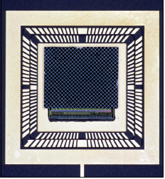
Illustration of a hybrid pixel detector. It comprises 3 components: a segmented sensor chip connected using solder balls to an identically segmented readout chip.
Thanks to the LAA initiative that lasted until the end of '90's and the launch of the R&D programme for the LHC detectors in 1990, novel technologies and prototypes that could operate in the harsh conditions of the LHC were introduced. At the same time, as the circuits were becoming more sophisticated and highly complex one should keep the operating power and the investment cost to an affordable size.
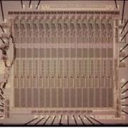
In 1998 the AMPLEX chip for multiplexed read-out allowed the UA2 experiment to employ an inner silicon-pad detector (left).By 2002, CERN had developed a bump-bonded 8000-channel silicon-pixel array (right) for the ALICE silicon-pixel detector at the LHC.
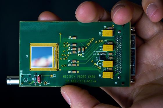
View of the Medipix Card built with an hybrid silicon pixel detectors for tracking applications in High Energy Physics and for imaging applications.
The members of the CERN microelectronics group proposed the use of full custom-design techniques that eventually led to the production of chips capable of copying with the extreme conditions at the LHC. The LHC experiments are based on sophisticated chips that can handle unprecedented event rates: 40 million pictures recorded per second, continuously. Moreover, some of the chips, or the underlying ideas that led to their development, find applications in material analysis, medical imaging or other types of industrial equipment.
Read also:
Designign pixel readout chips at CERN: From dream to reality. (PH newsletter, http://ep-news.web.cern.ch/content/designing-pixel-readout-chips-cern-dream-reality)
Microelectronics at CERN: from infancy to maturity (CERN Courier, March 2014).