![]()
HEP responds to the global chips crisis
Over the past year, semiconductor prices have been surging in Europe as demand increases globally. While this is happening with most products, it's been a larger problem given the role of semiconductors in most electronics, such as consumer electronics (smartphones, laptops, gaming consoles), automotive industry and home appliances. Coronavirus containment measures including lockdowns, led to a slowdown in manufacturing activities as factories remained closed over a long time while also led to a drop in the demand of semiconductor chips.
Following the gradual reopening of many economic activities, the global chip shortage was inevitable since the semiconductor industry was already operating at a fine balance of supply and demand. Coronavirus pandemic destabilized a market where a number of pre-existing factors were adding pressure to the supply chain including the growing demand for advanced chips used in AI and 5G-driven applications for cars, data centers and smartphones as well as the growing geopolitical tensions. A return to supply chain normality – with consumer electronics demand surging in response to changing consumer digital habits - doesn’t seem to be close, given the economic turbulence. According to a recent report, waiting times for new chips could be as long as 21 weeks, or around five months; one of the longest in the history of this industry.
Another factor contributing to the apparent crisis is the fact that, in the recent years the semiconductor fabrication companies (Figure 1) were concentrating in a race for developing ever more state-of-the art manufacturing processes and have not invested enough to increase manufacturing capacity for less advanced silicon chips used in numerus commodity electronics equipment and the automotive sector. Chips for the automotive sector are made using processes intended to meet safety criteria that are different from those meant for other industries and they are still fabricated on old process technologies used on 200-mm wafers. To reduce cost, the industry began moving to 300-mm wafers in 2000, but much of the old 200-mm infrastructure continued and even expanded. Despite the auto industry's desperation, there's no great rush to build new 200-mm fabs since the return on investment just isn't there yet. Therefore, chip shortage from 200-mm fabs is currently pronounced with a grim outlook for the coming two years.
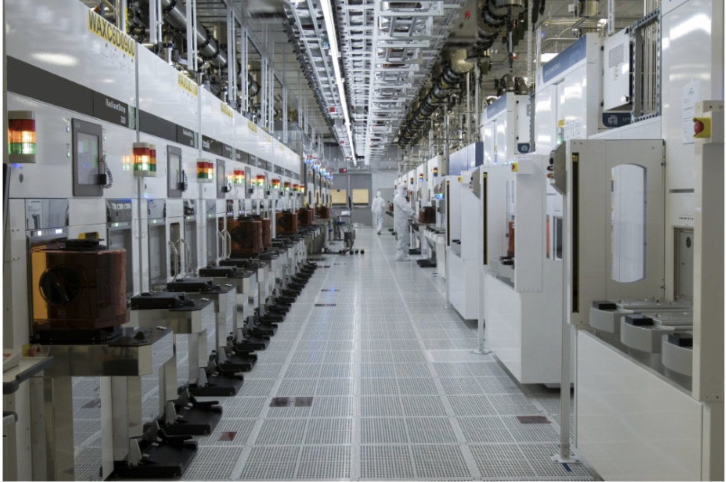
Figure 1. Clean room in semiconductor fabrication plant (foundry).
The chip shortage is happening simultaneously with national and regional efforts to boost advanced logic chip manufacturing. South Korea announced a push worth $450-billion until 2030, the United States is pushing legislation worth $52 billion until 2026, and the EU Chips Act proposal will plow more than EUR 43 billion up to 2030 into its semiconductor sector. China is accelerating efforts to close its technological gap and, by 2025 it is estimated that it will have invested around $150 billion over the past decade in line with a series of plans and initiatives such as the “Made in China 2025”. Political will to act quickly, together with the funding instruments and industry’s increased efforts could eventually lead to some isle of stability though the next period will remain rather volatile.
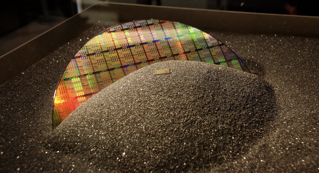
The global chip crisis, is also affecting research infrastructures as electronics is a critical component for most of the advanced scientific instrumentation and tools. All modern particle physics detectors make use of highly customized Application Specific Integrated Circuits (ASICs) for their operation. It should be noted that ASICs for scientific instrumentation represent a negligible fraction of the total semiconductors market and their availability can be compromised when the big players on the market are competing to reserve manufacturing capacity. Furtermore, a certain number of designs are still using 200-mm fabs and thus are affected by the pronounced manufacturing shortage.
CERN’s Foundry access and ASIC design support services
At CERN, since more than 20 years, the EP-ESE group (Electronic Systems for Experiments) supports the HEP community by providing access to mainstream semiconductor foundries for the prototyping and the production of ASIC designs as well as offering ASIC design support services to design teams. Foundry access services (see Figure 2), consists of establishing commercial contracts with the foundries and negotiating the legal frameworks that would permit collaborative work in the HEP community. ASIC design support services consists of the development of common design platforms that facilitate the collaborative work of distributed design teams working on common ASIC design projects. These services are complemented by direct technical support as well as training programmes offered to HEP engineers.
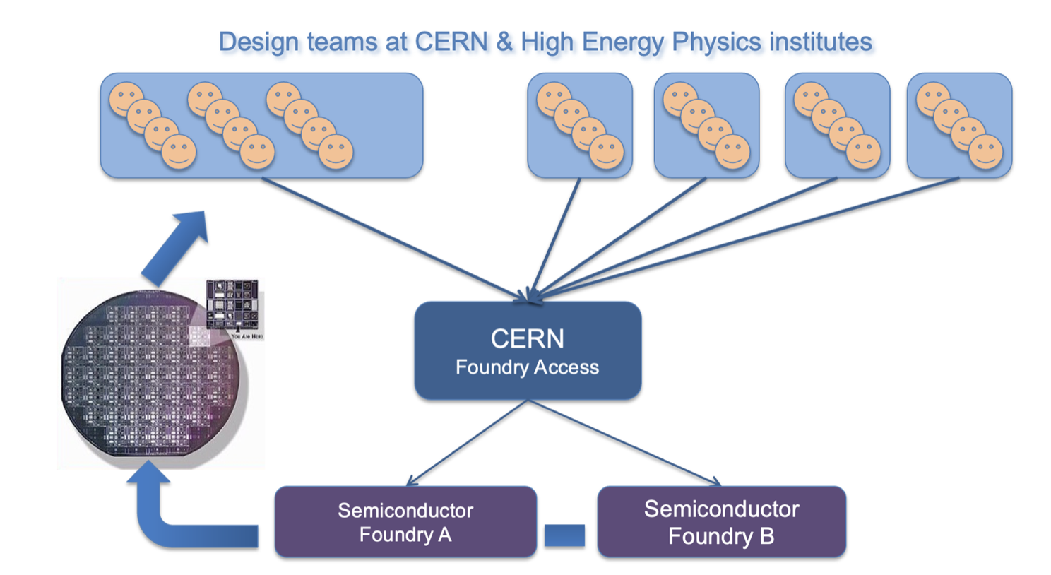
Figure 2. CERN's Foundry access services
Present challenges - shortage
Presently, CERN’s Foundry access service has two main semiconductor foundry suppliers for the planned HL-LHC detector upgrades who have both announced wafer capacity shortages extending throughout 2022-2023 as well as an increase in the manufacturing costs.
CERN and HEP institutes have access to the world’s largest and most advanced semiconductor foundry via the EUROPRACTICE service hosted at IMEC in Belgium. Access to advanced CMOS processes is essential for projects with the unique design characteristics such as those used in particle physics detectors. EUROPRACTICE is a long-standing key partner for CERN and the HEP community assuring the access to fabrication services under exclusive and preferential commercial conditions. CERN and HEP institutes have also a direct access to a second mainstream semiconductor foundry supplier. Over the years, CERN’s Foundry access service, has established excellent working relationships with both suppliers that proved to be extremely beneficial during the turmoil of the global chip crisis. CERN worked closely with both suppliers to mitigate the effects of the crisis finding ways to accommodate fabrication needs and to contain the increase in the fabrication costs.
At the advent of the chip crisis, the EP-ESE group reacted promptly, informing CERN management, the electronics coordinators of experiments and all ASIC design teams and project leaders about the looming difficulties. Subsequently, a survey of ASIC production needs among the detector development groups was launched and discussions with CERN’s main suppliers were initiated to find ways to accommodate the forecasted needs.
2021 was marked by intense prototyping and initial production activities for the LS3 upgrade program ASICs. CERN Foundry service in tight collaboration with HEP institutes ASIC design teams and close communications with foundry suppliers succeeded to obtain sufficient capacity to accommodate all LS3 production needs with a minimum cost impact.
This year, marks the entrance in “production years” for both ATLAS and CMS experiments. This translates to a total production volume of about 5000 wafers, a seemingly small quantity compared to the volumes attained in the silicon industry and yet a “high-volume” production with respect to the scientific instrumentation world. Clearly, the primary tool to mitigate the risks stemming from the present volatility is careful planning and smart thinking to maximize the available capacity.
Future prospects
As discussed, the global chip crisis is expected to continue well in 2022 and possibly beyond. The EP-ESE group will continue monitoring the situation, working closely with the experiments to follow up their needs, and coordinating with the foundry suppliers to mitigate the effects of the crisis in today’s dynamic environment. Despite the very tense situation and the announcement of further increase in production costs CERN will work with foundry suppliers to minimize the cost impact.