![]()
Pinpointing the structure of the SnV centre in diamond using emission channelling at ISOLDE
Diamond – beyond its allure as a jewel – exhibits an array of unique physical characteristics such as its hardness, the highest room thermal conductivity of any material (while being electrically insulating when undoped); it can also be doped to produce a variety of conducting states including superconductivity. These physical characteristics have raised the interest in exploiting the material for a variety of applications and diamond is now being utilised in a wide variety of areas ranging from electrochemical sensors, heat transport in high power infrared lasers, high resolution magnetometers and electronics. Impurities and defects in the diamond lattice influence directly the physical characteristics of the bulk material and understanding the structure and electronic nature of these defects leads directly to new areas of application.
A more recent area where diamond is being touted is in the realm of quantum information and optics. Negatively charge nitrogen-vacancy (NV-) centres in the diamond lattice have been the focus of intense research over the past 15 years and has been the most studied qubit in solid-state science. This has been due to the characteristics of the centre itself: its efficient optical spin polarisation and its long coherence time at room temperature. Nitrogen is also the dominant impurity in diamond and is thus relatively easy to control in terms of formation and which has been the subject of a vast amount of study in the last 50 years.
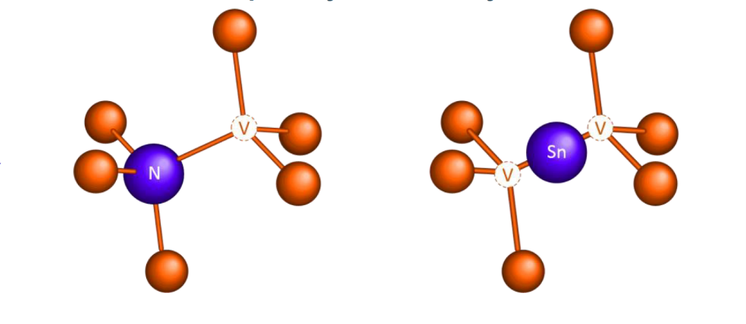
Figure 1: Examples of impurity-vacancy configurations in diamond. (a) NV on substitutional sites; (b) SnV centres in the “split vacancy” configuration.
In spite of the success enjoyed by the NV- centre, there are other examples of impurity vacancy centres which could be more suitable for future technologies. In particular, the group IV-V centres i.e. Si, Ge, Sn and Pb offer more efficient optical properties which are of special interest for nanophotonics due to their long spin coherence times. However, until recently many of the key properties and local configurations of these centres has remained unknown. Although space in the diamond lattice is limited, there are a variety of locations where impurities and defects can be accommodated and this can change considerably the bulk properties observed. Examples of two locations are shown in figure 1. The NV centre is known to occupy a substitutional lattice site with a neighbouring vacancy; the larger SnV system has been predicted to occupy a more spacious “split-vacancy” configuration. Knowledge of these local configurations is crucial to the successful exploitation of such centres which have to be created and controlled through ion implantation and subsequent thermal treatments. Recent work by the ECSLI (Emission channelling with short-lived isotopes) collaboration at ISOLDE has for the first time revealed the local structure of the SnV- centre using the technique of emission channelling [1].
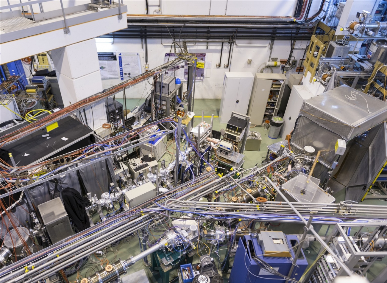
Emission channelling is a technique which allows the precise location of impurities in a crystalline lattice due to the emission of radioactive decay products e.g. alphas or in this case b-. Radioactive probes are implanted into the host lattice. During the measurement, the b- particles are channelled through or blocked by the potential of the host crystal’s lattice and are detected by a position sensitive Si detector. By recording decay patterns of emitted particles through a number of high symmetry directions a picture of the local environment where the implanted probes reside which are then compared to theoretical models to establish the nature of the detected patterns. The power of emission channelling in identifying lattice locations to a very high precision – a factor of 104 more efficient than traditional location techniques using external ion beams – is well known and has been used recently to identify the nature of Mg impurities in GaN [2]. Coupled to the wide number of available beams at the ISOLDE facility allows a wide variety of systems and materials to be studied.
Beams of 121Sn were produced at ISOLDE and implanted into a natural nitrogen-free diamond at 60kV. 121Sn decays with a half-life of 27.06h and measurements were collected. As a bonus, the long-lived metastable state of 121Sn (half-life =55 years) allowed optical measurements to be performed to investigate the luminescence properties of the implanted crystal.
A surprise was the large number of SnV- vacancy centres to occupy the configuration (b) shown in Figure 1: i.e. the split vacancy. Examples of the collected spectra and theoretical fits are shown in Figure 2 for as-implanted and annealed samples. Following annealing at 920C the number of channelling particles was found to double, indicating that damage was being annealed away or that Sn was undergoing a change of configuration in the lattice. This is supported by ab initio calculations but is the first direct experimental evidence for this structure involving Sn. Subsequent confocal photoluminescence spectroscopy revealed an order of magnitude higher optically active SnV- centres compared to previous results which appears to be explained by the absence of H – which alters charge states in the crystal – rendering the SnV- optically inactive by converting the centres to neutral SnV. This study has allowed for a detailed initial understanding of the formation processes for such centres in diamond and the role of diffusion of vacancies is now beginning to be understood as being crucial for the efficient production of optically active systems.
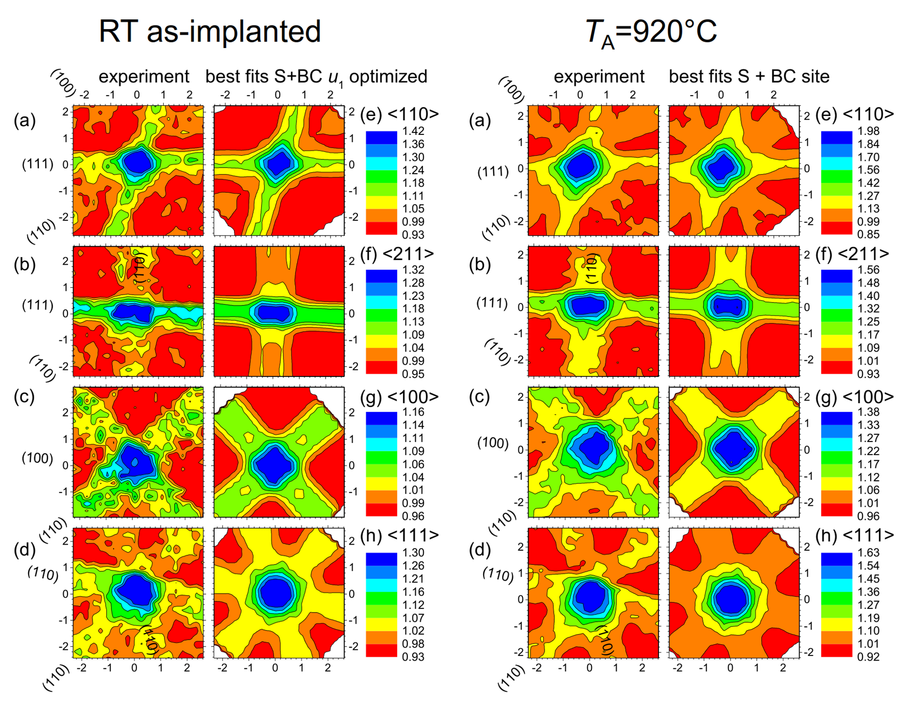
Figure 2 Channelling and fitting patterns for as-implanted Sn and annealing results for 920C.
This work has proved crucial in the understanding of the production mechanisms for centres well suited to nanophotonics applications. The aim of the collaboration will now be to extend these studies to other similar systems in diamond and to better correlate the local structure that emission channelling is so adept at unravelling to the optical centres that are studied by photoluminescence. A recent proposal to the INTC has been recommended for approval which continues this work with a goal to understanding in detail the optimal parameters for fabricating these centres and which will eventually lay the foundation for the exploitation of these centres for quantum communication applications.
References
[1] Wahl et al Physical review letters 125, 045301 (2020)
[2] Wahl et al Phys. Rev. Lett. 118, 095501