![]()
CHIPS: A new EP-ESE service for the HEP community
ASIC technology and designs are becoming increasingly complex but bring potentially huge benefits to HEP experiments (see also previous EP article "A bright future for microelectronics"). Figure 1 summarises the evolution of CMOS technologies in the last decades, and their increasingly delayed adoption in HEP. Each CMOS generation is identified by the minimum physical feature that can be produced in silicon, that is the minimum length of each MOS transistor. In our community, we are using today the 65nm generation, while industry is producing chips in the 7nm one, six generations ahead. With the decrease in the size, accompanied by a proportional saving in power consumption, the number of transistors that can be integrated on a single chip largely increases (see the dark blue line). In addition, reliably manufacturing multi-billion fully-functional transistors per chip requires many more processing steps, some of which beyond what could be imagined only a decade ago. This increased complexity in technology also affects circuit design, and as a consequence some HEP designs might be confronted with the tangible risk of failure or delay with potentially severe consequences on the physics programme.
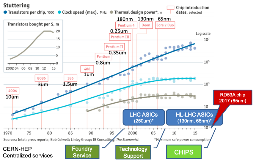
Figure 1: The evolution of microelectronics technology in the last decades is characterised by a steady decrease in MOS transistor size, that made it possible to increase the number and speed of transistors per chip and to lower their power consumption (taken from K. Kloukinas, 2019). HEP adopted the 250nm node in 1997-98 for the design of most of the ASICs now participating in the LHC data taking. CERN created a Foundry Service to assist the HEP community in the production of ASICs, which evolved into a more comprehensive Technology Support when our community moved to 130 and 65nm for circuits targeting the LHC and HL-LHC upgrades. Meanwhile, industry is now manufacturing the most advanced chips 6 generations ahead, in the 7nm node.
The new and more sophisticated design tools and design flows that are now available to ASIC designers must be used in these technologies. As a community, we have to face the challenges associated with the new level of design and verification complexity. This means developing and following scrupulously the Digital-on-Top design methodology. In this methodology, a fully scripted automated flow is used to drive the digital tools to design and implement the digital circuitry around the analog blocks. This flow facilitates the top-level architectural design, which can be emulated and verified using Universal Verification Methodology (UVM), simulation and functional verification, floor planning and power planning, logic synthesis, cell placement and signal routing, timing analysis, physical verification and power analysis. This flow is particularly adapted for large and complex designs implemented in advanced very deep submicron technologies. It requires perhaps an order of magnitude more effort than the Analog-on-Top approach but, where carefully followed, it strongly mitigates the risk of a failed design.
As a community we are already benefiting from the careful and thorough adoption of such techniques in the preparation of designs for the HL-LHC upgrades. Examples include developments for several experiment-dedicated and common chips. However, these techniques are still not applied systematically to all large scale ASIC designs for HEP experiments. In an attempt to facilitate the adoption of these modern design techniques, a new CERN-HEP IC design Platform and Services (CHIPS) activity has been started in the Microelectronics Section of the ESE group at CERN in January 2020, for an initial duration of 5 years.
The EP-ESE-ME already supports the HEP community with common design platforms and standardized design techniques since 2008 through the ASIC Technology Support and Foundry Services platform (https://espace.cern.ch/asics-support) led by Kostas Kloukinas. However, the amount of support provided is strongly constrained by an organizational structure where the support depends on a very small group of individuals. The CHIPS project is a new activity within EP-ESE-ME to further extend the support and encompass ASIC design and verification. The action plan has three main points:
-
To involve design and verification experts in the support. While at present only a small core team in the EP-ESE-ME section provides support, the new initiative foresees to redistribute the technical support tasks that can only be provided by experienced practitioners more uniformly across the designers in the section. For each step in the design flow one or two specialists will be identified and these will be tasked with supporting outside groups.
-
To extend the subcontract of specialized tasks outside CERN, reinforcing contracts with companies able to give punctual help with particular issues related to the tools and design flow. These facilities should be available both to CERN engineers and to members of the community. As with all such external contracts there should be one person responsible (of course with a back-up) to act as intermediary between the company and the designers.
-
To train and coach. Continue to organize formal training sessions to expose designers to the latest tools and, in particular, to educate them in the use of the common design platform. Furthermore, the initiative foresees the creation of ‘hot desks’ at CERN that could be allocated to host designers from the HEP community for several months. This would considerably favor exchanges and contribute to increase the shared expertise in the community.
A diagram of the CHIPS activity organization is shown below. Xavier Llopart is the appointed CHIPS Project Manager. With the help of the ME Section Leader, the CHIPS Project Manager will receive the support requests (chips.support@cern.ch), propose the most suitable solution (direct support, on-the-job training, specialised contract), and coordinate its implementation. The CHIPS service framework has now been launched. First requests are being received, and support solutions are being analysed. In time, this initiative should help design teams in the HEP community to achieve first-silicon success using modern high performance but expensive technologies. This goal will be reached by providing design support and diffusing expertise across the HEP community, where design teams are scattered and often composed of a very small number of practitioners that can not specialise in all the steps and tools necessary for the design of complex chips.
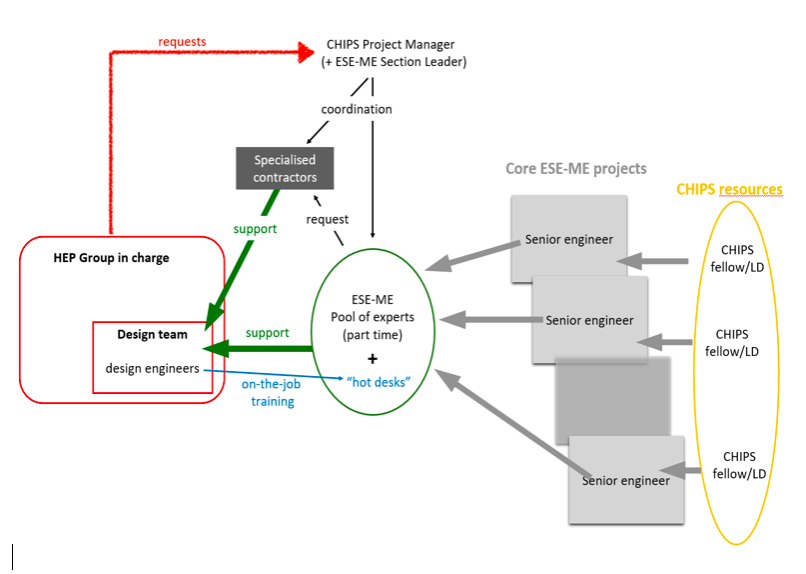
Figure 2: The organization of the CHIPS initiative foresees a central pool of expert practitioners from the core EP-ESE-ME projects. Under the coordination of a Project Manager, support to the HEP groups in charge for the ASIC design can be provided in different forms.