
Tag: ASICs
-

A Hundred Gigabits per Fibre: Silicon Photonics Links for the Detectors of Tomorrow
The High-Speed Links Work Package (WP6) of the EP R&D programme is developing the radiation-tolerant, high-bandwidth optical links needed for future particle detectors. Combining custom ASICs, Silicon Photonics and FPGA-based back-end systems, the team is now moving towards integrated demonstrations in an experimental context.
-
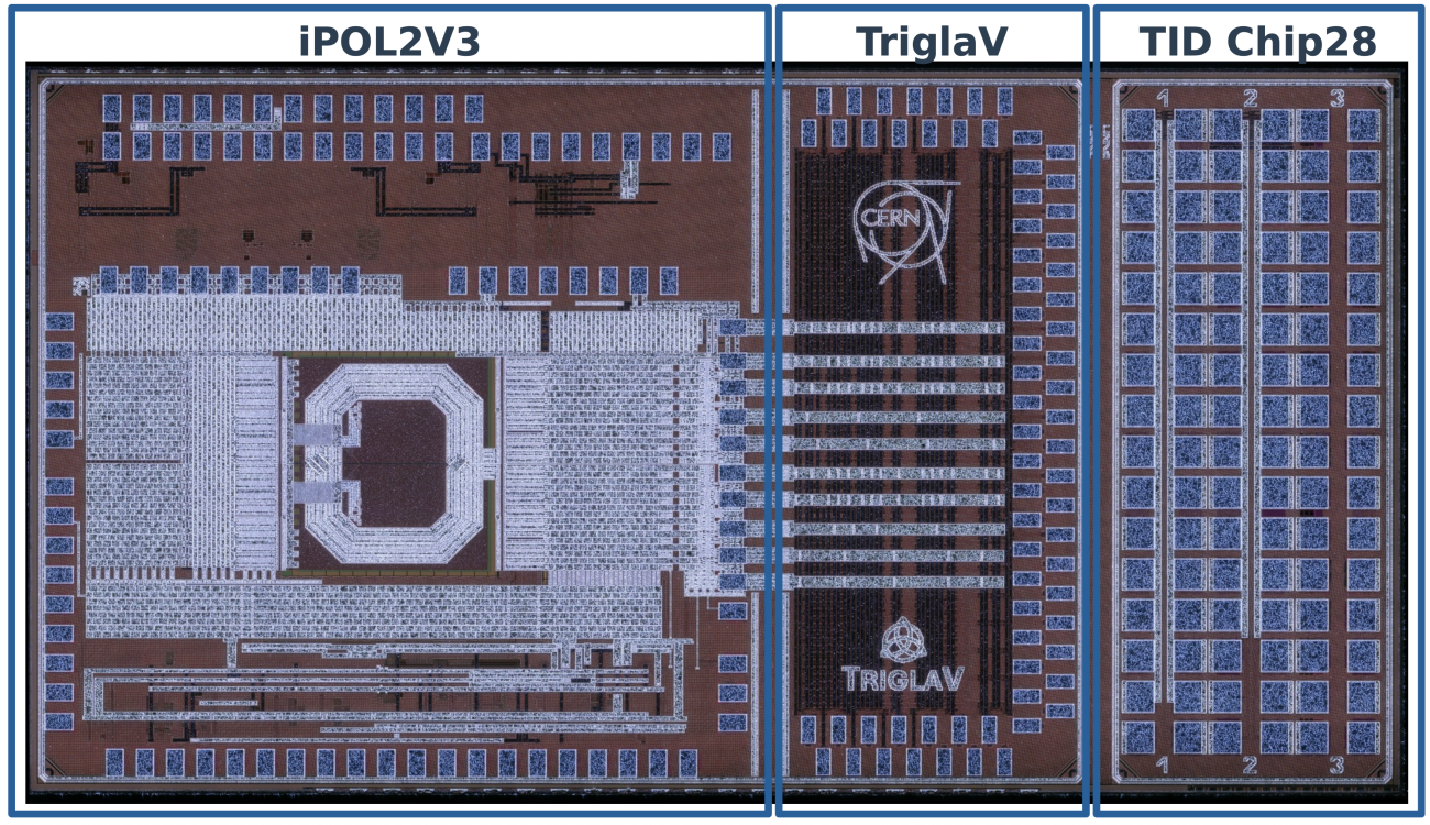
Building a Microelectronics Foundation for Tomorrow’s Detectors
Building a Microelectronics Foundation for Tomorrow’s Detectors The challenge: smarter chips in harsher places Particle physics detectors have always pushed electronics to their limits. The next generation of tracking systems and calorimeters will depend critically on dense, intelligent, low power and radiation-hard microelectronics: front-end ASICs that can survive for decades in harsh environments, having their
-
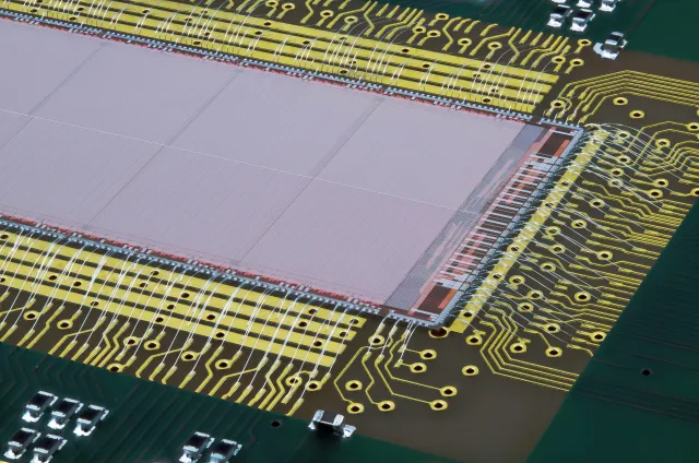
MOSAIX: Designing bent wafer-scale monolithic pixel sensors for the ALICE ITS3 upgrade
MOSAIX: Designing bent wafer-scale monolithic pixel sensors for the ALICE ITS3 upgrade The ALICE detector is preparing a major upgrade to its Inner Tracking System (ITS) during LHC long shutdown 3 (2026-2030). This upgrade, called ITS3, will replace the three innermost tracking layers with three layers of cylindrical, 50 µm thick, 27 cm long, silicon
-
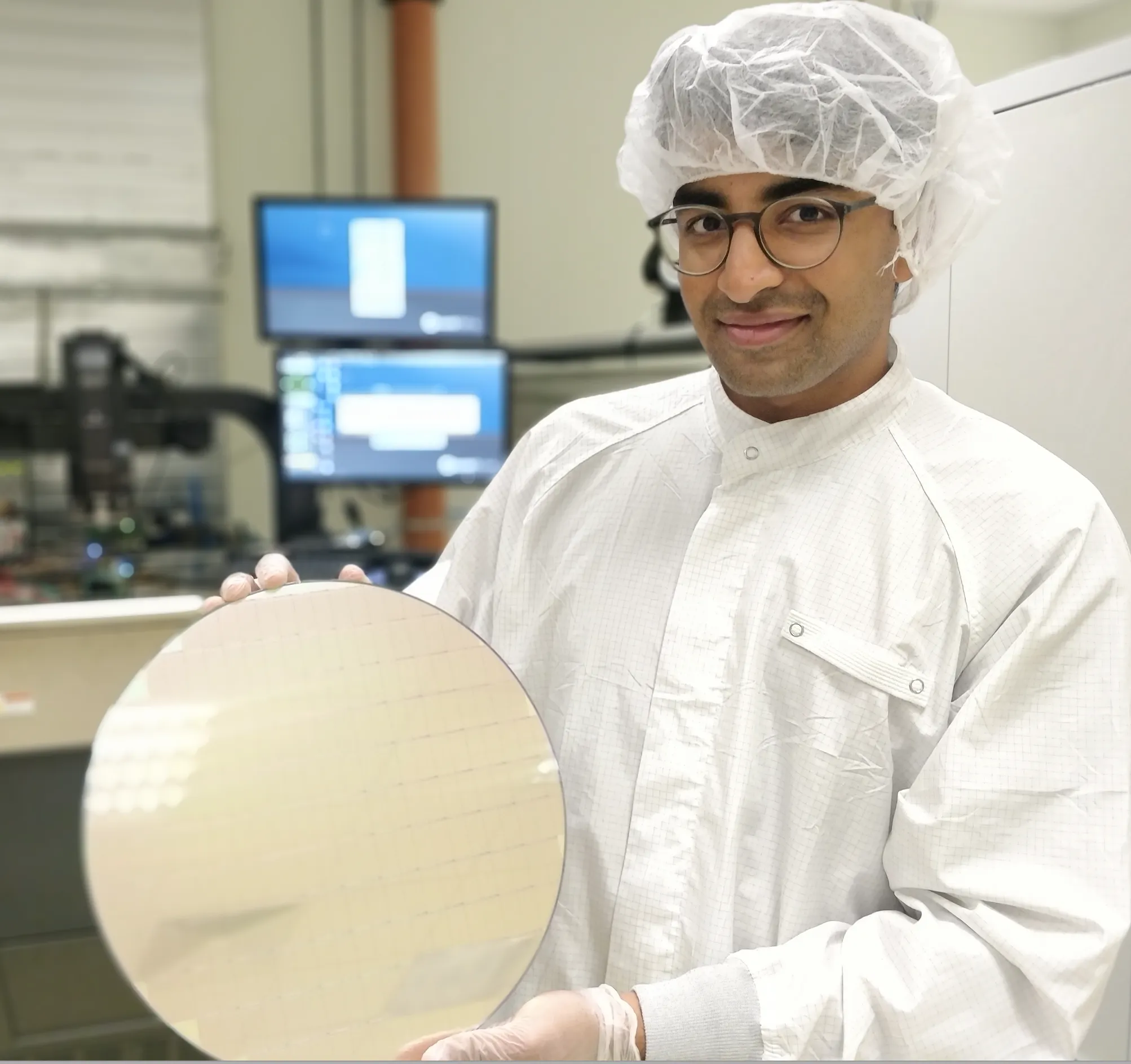
Wafer-level testing of CMS Outer Tracker ASICs
Wafer-level testing of CMS Outer Tracker ASICs The Macro-Pixel ASIC (MPA) and Short-Strip ASIC (SSA) are the new read-out chips used to process particle hit signals of pixel and strip sensors in the upcoming CMS Outer Tracker of the High-Luminosity LHC Upgrade (HL-LHC). The two chips are produced by TSMCs 65nm fabrication process and were
-
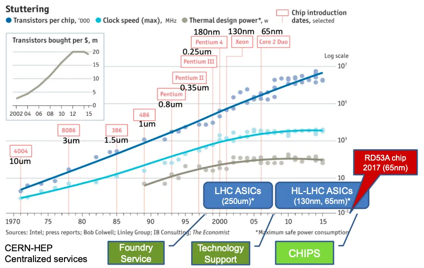
CHIPS: A new EP-ESE service for the HEP community
CHIPS: A new EP-ESE service for the HEP community ASIC technology and designs are becoming increasingly complex but bring potentially huge benefits to HEP experiments (see also previous EP article “A bright future for microelectronics“). Figure 1 summarises the evolution of CMOS technologies in the last decades, and their increasingly delayed adoption in HEP. Each