![]()
ALICE ITS3 clears major milestone
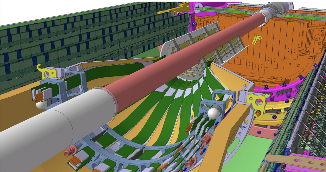
With the R&D for the first truly cylindrical detectors based on ultra-thin, bent, wafer-scale monolithic silicon sensors, the ALICE collaboration aims at installing new vertex layers (“ITS3”) in LHC Long Shutdown 3. The envisioned setup comprises 6 Monolithic Active Pixel Sensors (MAPS) of more than 20 cm lengths arranged in three layers and held in place with carbon foam (Fig. 1). It will have a material budget of below 0.05% X0 or about 1/10th of the current layers. The Letter of Intent [1] was presented to the LHCC in September 2019, and following the endorsement [2] an intense R&D period started. Recently, a summary on the project status was given at the CERN detector seminar [3] from which a few key points are summarised here.
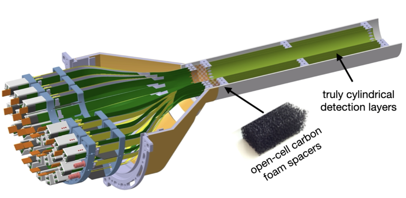
Figure 1. Proposed detector layout. The full detector is based on two of these halves, with layers at radii of 18, 24, and 30 mm surrounding the beam pipe. Note that a single piece of silicon is used to equip a full half-layer, meaning that the total detector comprises six sensors only.
A set of important milestones has since been addressed, the first being the validation of bent Monolithic Active Pixel Sensors (MAPS) in beam. Here, a first demonstration was done at DESY in June 2020 [4] using 50 μm thick ALPIDE chips that are used in the recently installed tracker (“ITS2”, [5]). The excellent performance figures of ALPIDE were retained after bending (Fig. 2), proving that highly non-planar geometries become possible profiting from the flexible nature of thin silicon. The bending technique has been optimised and several prototypes of bent detectors were brought to beam tests at DESY and CERN (PS and SPS), including a setup with 3 layers of ALPIDEs at the target radii of ITS3, called “μITS3” (Fig. 3).
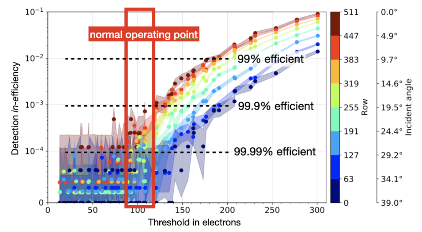
Figure 2. Results for the first (June 2020 DESY) beam with an ALPIDE chip [3], showing that the sensor remains 100% efficient after bending to radii of 2 cm.
Figure 3. The “μITS3” assembly, based on 6 ALPIDE chips that are bent to the target radii of ITS3 (2 chips each at 18, 24, and 30 mm).
At the same time, mechanical studies on wafer-scale silicon dummies were carried out and resulted in a first full-sized mock-up of a half-cylinder (Fig. 4), which allow the study of geometrical precision, air-cooling performance and production processes. In particular, the selection of the carbon foam material has been finalised and the bending and gluing procedures were optimised.
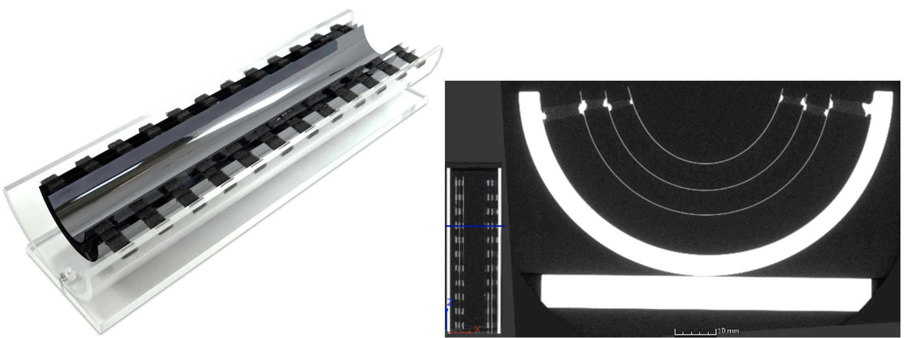
Figure 4: Fully assembled detector half based on 40 and 50 μm thick dummy silicon pieces (left) and 3D Xray scan (right). The latter shows a small glue spillage at the interfaces of the chips to the carbon foam retaining pieces, whose reduction is ongoing now.
More recently, late summer 2021, the chips from the first submission in the target silicon technology, TPSCo 65nm, became available for tests. With respect to the 180 nm CMOS Image Sensor technology of TowerJazz in which the ALPIDE sensors of ITS2 [5] were developed, the new technology offers not only higher integration density and possibly lower power consumption, but is also done on larger wafers (300 mm instead of 200 mm), allowing the production of longer sensors – long enough to equip a full half-layer for ALICE.
The chips, that were designed in the framework of CERN EP R&D WP1.2, include a number of test structures to address the radiation hardness of the technology as well as its charge collection properties. The first measurements are very positive, in particular showing that particle detection performance is 100%. Ongoing tests with irradiated samples give indications that these figures are retained at the radiation levels expected at ALICE in Run 4.
As a particular highlight, test structures (“DPTS”), comprising 32 by 32 pixels in 15 μm pitch, and including a complete digital front-end were characterised in a beam tests at DESY for their detection performance. An exemplary result (Fig. 5) shows the detection efficiency of 100%. These results are now being further substantiated with the analysis of larger data samples and are now also accompanied by test of samples after irradiation.
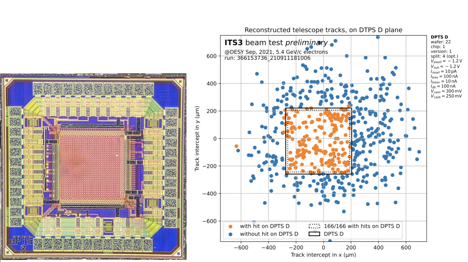
Figure 5: The DPTS chip (left) and its beam test results from DESY (September 2021, right). The round markers show the impinging point of beam particles as reconstructed by a beam telescope at the plane where the DPTS chip is placed. They are coloured orange if they produce a hit in the DTPS. It can clearly be seen that all particles crossing the sensor, also produce a hit, meaning that it detects all particles.
In conclusion, the first two years of R&D resulted in a number of important results, such as the qualification of a target technology, demonstration of the feasibility of the thinning and bending process and the mechanical integration and cooling process, paving the road for the development of a new class of detectors with non-planar optimised geometries and minimal material budgets. The collaboration is eagerly looking forward towards the next steps, namely the production of the first wafer-scale sensors and their integration.
References
[1] LoI: CERN-LHCC-2019-018 (LHCC-I-034).
[2] LHCC minutes,139th meeting CERN-LHCC-2019-010 (LHCC-139)
[3] ALICE ITS3 – a next generation vertex detector based on bent, wafer-scale CMOS sensors (https://indico.cern.ch/event/1071914/)
[4] First demonstration of in-beam performance of bent Monolithic Active Pixel Sensors (arXiv:2105.13000).
[5] The ALICE ITS upgrade: Pixels for quarks (EP Newsletter, September 2019)